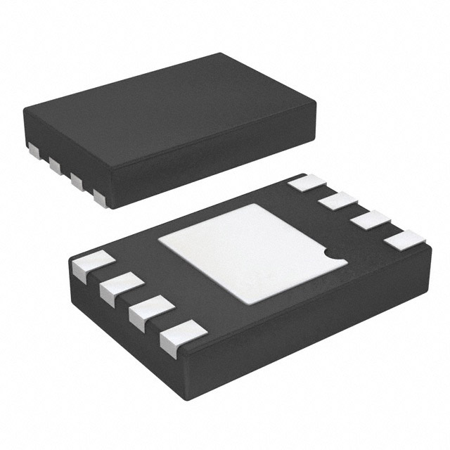
BD3539NUX-TR
Active1A VARIABLE OUTPUT TERMINATION REGULATOR FOR DDR-SDRAMS
Deep-Dive with AI
Search across all available documentation for this part.

BD3539NUX-TR
Active1A VARIABLE OUTPUT TERMINATION REGULATOR FOR DDR-SDRAMS
Deep-Dive with AI
Technical Specifications
Parameters and characteristics for this part
| Specification | BD3539NUX-TR |
|---|---|
| Applications | Converter, DDR SDRAM |
| Mounting Type | Surface Mount |
| Number of Outputs | 1 |
| Operating Temperature [Max] | 100 °C |
| Operating Temperature [Min] | -30 ░C |
| Package / Case | 8-UFDFN Exposed Pad |
| Supplier Device Package | VSON008X2030 |
| Voltage - Input [Max] | 5.5 V |
| Voltage - Input [Min] | 2.7 V |
| Voltage - Output | Adjustable |
Pricing
Prices provided here are for design reference only. For realtime values and availability, please visit the distributors directly
| Distributor | Package | Quantity | $ | |
|---|---|---|---|---|
| Digikey | Cut Tape (CT) | 1 | $ 2.08 | |
| 10 | $ 1.33 | |||
| 25 | $ 1.13 | |||
| 100 | $ 0.91 | |||
| 250 | $ 0.80 | |||
| 500 | $ 0.73 | |||
| 1000 | $ 0.68 | |||
| Digi-Reel® | 1 | $ 2.08 | ||
| 10 | $ 1.33 | |||
| 25 | $ 1.13 | |||
| 100 | $ 0.91 | |||
| 250 | $ 0.80 | |||
| 500 | $ 0.73 | |||
| 1000 | $ 0.68 | |||
| N/A | 3909 | $ 1.22 | ||
| Tape & Reel (TR) | 4000 | $ 0.44 | ||
| Newark | Each (Supplied on Cut Tape) | 1 | $ 1.45 | |
| 10 | $ 1.11 | |||
| 25 | $ 1.00 | |||
| 50 | $ 0.89 | |||
| 100 | $ 0.79 | |||
| 250 | $ 0.75 | |||
| 500 | $ 0.71 | |||
| 1000 | $ 0.65 | |||
Description
General part information
BD3539 Series
BD3539FVM is a termination regulator that complies with JEDEC requirements for DDR1-SDRAM, DDR2-SDRAM, and DDR3-SDRAM. This linear power supply uses a built-in N-channel MOSFET and high-speed OP-AMPS specially designed to provide excellent transient response. It has a sink/source current capability of up to 1A and has a power supply bias requirement of 3.3 V (for DDR2 and DDR3) and 5.0 V (for DDR1, DDR2, and DDR3) for driving the N-channel MOSFET. By employing an independent reference voltage input (VDDQ) and a feedback pin (VTTS), this termination regulator provides excellent output voltage accuracy and load regulation as required by JEDEC standards. Additionally, BD3539 has a reference power supply output (VREF)for DDR-SDRAM or for memory controllers. Unlike the VTT output that goes to "Hi-Z" state, the VREF output is kept unchanged when EN input is changed to "Low", making this IC suitable for DDR-SDRAM under "Self Refresh" state.
Documents
Technical documentation and resources


