Deep-Dive with AI
Search across all available documentation for this part.

Deep-Dive with AI
Technical Specifications
Parameters and characteristics for this part
| Specification | CD40147BM96G4 |
|---|---|
| Circuit [custom] | 1 |
| Circuit [custom] | 10:4 |
| Current - Output High, Low [custom] | 6.8 mA |
| Current - Output High, Low [custom] | 6.8 mA |
| Independent Circuits | 1 |
| Mounting Type | Surface Mount |
| Operating Temperature [Max] | 125 °C |
| Operating Temperature [Min] | -55 °C |
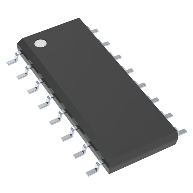
| Package / Case | 16-SOIC |
| Package / Case [x] | 0.154 in |
| Package / Case [y] | 3.9 mm |
| Supplier Device Package | 16-SOIC |
| Type | Priority Encoder |
| Voltage - Supply [Max] | 18 V |
| Voltage - Supply [Min] | 3 V |
| Voltage Supply Source | Single Supply |
Pricing
Prices provided here are for design reference only. For realtime values and availability, please visit the distributors directly
| Distributor | Package | Quantity | $ | |
|---|---|---|---|---|
Description
General part information
CD40147B Series
The CD40147B CMOS encoder features priority encoding of the inputs to ensure that only the highest-order data line is encoded. Ten data input lines (0-9) are encoded to four-line (8, 4, 2, 1) BCD. The highest priority line is line 9. All four output lines are logic 1 (VSS) when all input lines are logic 0. All inputs and outputs are buffered, and each output can drive one TTL low-power Schottky load. The CD40147B is functionally similar to the TTL54/74147 if pin 15 is tied low.
The CD40147B types are supplied in 16-lead dual-in-line plastic packages (E suffix), 16-lead small-outline packages (M, M96, MT and NSR suffixes), and 16-lead thin shrink small-outline packages (PW and PWR suffixes).
The CD40147B CMOS encoder features priority encoding of the inputs to ensure that only the highest-order data line is encoded. Ten data input lines (0-9) are encoded to four-line (8, 4, 2, 1) BCD. The highest priority line is line 9. All four output lines are logic 1 (VSS) when all input lines are logic 0. All inputs and outputs are buffered, and each output can drive one TTL low-power Schottky load. The CD40147B is functionally similar to the TTL54/74147 if pin 15 is tied low.
Documents
Technical documentation and resources
No documents available


