Zenode.ai Logo
Beta
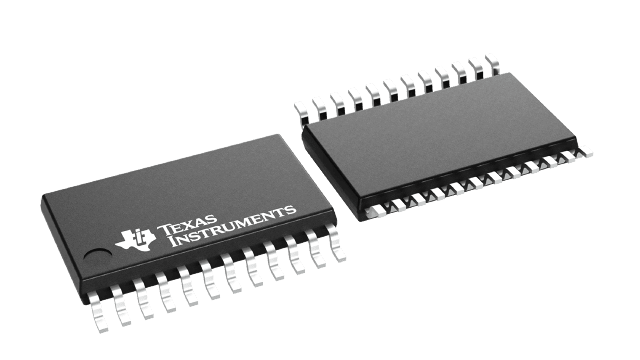
TSSOP (PW)
Integrated Circuits (ICs)

SN74LVC841APW

Active
Texas Instruments

10-BIT BUS-INTERFACE D-TYPE LATCH WITH 3-STATE OUTPUTS

Deep-Dive with AI

Search across all available documentation for this part.

TSSOP (PW)
Integrated Circuits (ICs)

SN74LVC841APW

Active
Texas Instruments

10-BIT BUS-INTERFACE D-TYPE LATCH WITH 3-STATE OUTPUTS

Technical Specifications

Parameters and characteristics for this part

SpecificationSN74LVC841APW
Circuit10:10
Current - Output High, Low24 mA
Delay Time - Propagation2.7 ns
Independent Circuits1
Logic TypeD-Type Transparent Latch
Mounting TypeSurface Mount
Operating Temperature [Max]85 °C
Operating Temperature [Min]-40 °C
Output TypeTri-State
Package / Case24-TSSOP
Package / Case0.173 in, 4.4 mm
Supplier Device Package24-TSSOP
Voltage - Supply [Max]3.6 V
Voltage - Supply [Min]1.65 V

Pricing

Prices provided here are for design reference only. For realtime values and availability, please visit the distributors directly

DistributorPackageQuantity$
DigikeyTube 600$ 1.61
Texas InstrumentsTUBE 1$ 2.04
100$ 1.69
250$ 1.21
1000$ 0.91

Description

General part information

SN74LVC841A Series

This 10-bit bus-interface D-type latch is designed for 1.65-V to 3.6-V VCCoperation.

The SN74LVC841A is designed specifically for driving highly capacitive or relatively low-impedance loads. It is particularly suitable for implementing buffer registers, I/O ports, bidirectional bus drivers, and working registers.

The ten latches are transparent D-type latches. The device has noninverting data (D) inputs and provides true data at its outputs.

Documents

Technical documentation and resources

Low-Voltage Logic (LVC) Designer's Guide

Design guide

Bus-Interface Devices With Output-Damping Resistors Or Reduced-Drive Outputs (Rev. A)

Application note

LOGIC Pocket Data Book (Rev. B)

User guide

SN74LVC841A datasheet (Rev. J)

Data sheet

Migration From 3.3-V To 2.5-V Power Supplies For Logic Devices

Application note

Texas Instruments Little Logic Application Report

Application note

Design Summary for WCSP Little Logic (Rev. B)

Product overview

Implications of Slow or Floating CMOS Inputs (Rev. E)

Application note

LVC and LV Low-Voltage CMOS Logic Data Book (Rev. B)

User guide

Signal Switch Data Book (Rev. A)

User guide

Live Insertion

Application note

Selecting the Right Level Translation Solution (Rev. A)

Application note

LVC Characterization Information

Application note

Little Logic Guide 2018 (Rev. G)

Selection guide

Power-Up 3-State (PU3S) Circuits in TI Standard Logic Devices

Application note

Understanding Advanced Bus-Interface Products Design Guide

Application note

16-Bit Widebus Logic Families in 56-Ball, 0.65-mm Pitch Very Thin Fine-Pitch BGA (Rev. B)

Application note

Standard Linear & Logic for PCs, Servers & Motherboards

More literature

STANDARD LINEAR AND LOGIC FOR DVD/VCD PLAYERS

More literature

Power-Up Behavior of Clocked Devices (Rev. B)

Application note

Understanding and Interpreting Standard-Logic Data Sheets (Rev. C)

Application note

Use of the CMOS Unbuffered Inverter in Oscillator Circuits

Application note

Logic Guide (Rev. AB)

Selection guide

How to Select Little Logic (Rev. A)

Application note

CMOS Power Consumption and CPD Calculation (Rev. B)

Application note

TI IBIS File Creation, Validation, and Distribution Processes

Application note

Input and Output Characteristics of Digital Integrated Circuits

Application note

Semiconductor Packing Material Electrostatic Discharge (ESD) Protection

Application note