BD35390FJ-E2
Active1A VARIABLE OUTPUT TERMINATION REGULATOR FOR DDR-SDRAMS
Deep-Dive with AI
Search across all available documentation for this part.

BD35390FJ-E2
Active1A VARIABLE OUTPUT TERMINATION REGULATOR FOR DDR-SDRAMS
Technical Specifications
Parameters and characteristics for this part
| Specification | BD35390FJ-E2 |
|---|---|
| Applications | DDR Bus Termination Regulator, Converter |
| Mounting Type | Surface Mount |
| Number of Outputs | 1 |
| Operating Temperature [Max] | 100 °C |
| Operating Temperature [Min] | -30 ░C |
| Package / Case | 0.154 in |
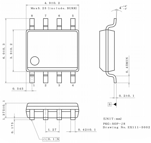
| Package / Case | 8-SOIC |
| Package / Case | 3.9 mm |
| Supplier Device Package | 8-SOP-J |
| Voltage - Input [Max] | 5.5 V |
| Voltage - Input [Min] | 2.7 V |
| Voltage - Output | Multiple |
Pricing
Prices provided here are for design reference only. For realtime values and availability, please visit the distributors directly
| Distributor | Package | Quantity | $ | |
|---|---|---|---|---|
| Digikey | N/A | 0 | $ 0.63 | |
Description
General part information
BD35390FJ Series
BD35390FJ is a termination regulator that complies with JEDEC requirements for DDR1/2/3-SDRAM. This linear power supply uses a built-in N-channel MOSFET and high-speed OP-AMPS specially designed to provide excellent transient response. It has a sink/source current capability up to 1A and has a power supply bias requirement of 3.3V to 5.0V for driving the N-channel MOSFET. By employing an independent reference voltage input (VDDQ) and a feedback pin (VTTS), this termination regulator provides excellent output voltage accuracy and load regulation as required by JEDEC standards.
Documents
Technical documentation and resources


