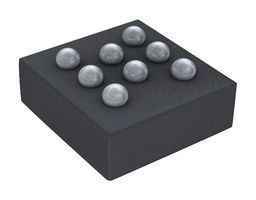
NB3RL02FCT2G
ActiveCLOCK BUFFER, FANOUT, 9 MHZ TO 80 MHZ, 2 OUTPUTS, 2.3 V TO 5.5 V, 8 PINS, WLCSP
Deep-Dive with AI
Search across all available documentation for this part.

NB3RL02FCT2G
ActiveCLOCK BUFFER, FANOUT, 9 MHZ TO 80 MHZ, 2 OUTPUTS, 2.3 V TO 5.5 V, 8 PINS, WLCSP
Deep-Dive with AI
Technical Specifications
Parameters and characteristics for this part
| Specification | NB3RL02FCT2G |
|---|---|
| Differential - Input:Output | False |
| Frequency - Max [Max] | 52 MHz |
| Input | Clock |
| Mounting Type | Surface Mount |
| Number of Circuits | 1 |
| Operating Temperature [Max] | 85 °C |
| Operating Temperature [Min] | -40 °C |
| Output | LVCMOS |
| Package / Case | 8-XFBGA, WLCSP |
| Ratio - Input:Output [custom] | 1:2 |
| Supplier Device Package | 8-WLCSP (1.57x0.77) |
| Supplier Device Package [x] | 1.57 |
| Supplier Device Package [y] | 0.77 |
| Type | Fanout Buffer (Distribution) |
| Voltage - Supply [Max] | 5.5 V |
| Voltage - Supply [Min] | 2.3 V |
Pricing
Prices provided here are for design reference only. For realtime values and availability, please visit the distributors directly
Description
General part information
NB3RL02 Series
The NB3RL02 is a low-skew, low jitter 1:2 clock fan-out buffer, ideal for use in portable end-equipment, such as mobile phones. With integrated LDO and output control circuitry. The MCLK_IN pin has an AC coupling capacitor and will directly accept a square or sine wave clock input, such as a temperature compensated crystal oscillator (TCXO). The minimum acceptable input amplitude of the sine wave is 300 mV peak-to-peak. The two clock outputs are enabled by control inputs CLK_REQ1 and CLK_REQ2. The NB3RL02 has an integrated Low-Drop-Out (LDO) voltage regulator which accepts input voltages from 2.3 V to 5.5 V and outputs 1.8 V at Iout = 50 mA. This 1.8 V supply is externally available to provide regulated power to peripheral devices, such as a TCXO. The adaptive clock output buffers offer controlled slew-rate over a wide capacitive loading range which minimizes EMI emissions, maintains signal integrity, and minimizes ringing caused by signal reflections on the clock distribution lines. The NB3RL02 is offered in a 0.4 mm pitch wafer-level-chip-scale (WLCS) package (0.77 mm x 1.57 mm) and is optimized for very low standby current consumption.
Documents
Technical documentation and resources


