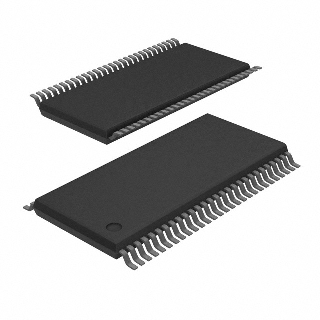
SN75LBC968DL
Active9-CHANNEL BUS TRANSCEIVER WITH ACTIVE TERMINATION
Deep-Dive with AI
Search across all available documentation for this part.

SN75LBC968DL
Active9-CHANNEL BUS TRANSCEIVER WITH ACTIVE TERMINATION
Deep-Dive with AI
Technical Specifications
Parameters and characteristics for this part
| Specification | SN75LBC968DL |
|---|---|
| Duplex | Half |
| Mounting Type | Surface Mount |
| Number of Drivers/Receivers [custom] | 9 |
| Number of Drivers/Receivers [custom] | 9 |
| Operating Temperature [Max] | 70 °C |
| Operating Temperature [Min] | 0 °C |
| Package / Case | 0.295 in |
| Package / Case | 56-BSSOP |
| Package / Case | 7.5 mm |
| Receiver Hysteresis | 500 mV |
| Supplier Device Package | 56-SSOP |
| Type | Transceiver |
| Voltage - Supply [Max] | 5.25 V |
| Voltage - Supply [Min] | 4.75 V |
Pricing
Prices provided here are for design reference only. For realtime values and availability, please visit the distributors directly
| Distributor | Package | Quantity | $ | |
|---|---|---|---|---|
| Digikey | Tube | 60 | $ 18.86 | |
| Texas Instruments | TUBE | 1 | $ 20.88 | |
| 100 | $ 18.24 | |||
| 250 | $ 14.06 | |||
| 1000 | $ 12.58 | |||
Description
General part information
SN75LBC968 Series
The SN75LBC968 is a nine-channel transceiver with active termination that drives and receives the signals from the single-ended, parallel data buses such as the Small Computer-Systems Interface (SCSI) bus. The features of the line drivers, receivers, and active-termination circuits provide the optimum signal-to-noise ratios for reliable data transmission. Integration of the termination and transceivers in the LinBiCMOS™ process provides the necessary analog-circuit performance, has low quiescent power, and reduces the capacitance presented to the bus over separate termination and I/O circuits.
The transceivers of the SN75LBC968 can be enabled to function as totem-pole or open-drain outputs. The open-drain mode drives the wired-OR lines of SCSI (BSY, SEL, and RST) by inputting the data to the direction control input DE/RE instead of the A input. When driving the data through the A input, the outputs become totem poles and provide active signal negation for a higher voltage level on low-to-high signal transitions on heavily loaded buses. In either mode, the turnon and turnoff output transition times are limited to minimize crosstalk through capacitive coupling to adjacent lines and RF emissions from the cable. The receivers are also designed for optimum analog performance by precisely controlling the input-voltage thresholds, providing wide input-voltage hysteresis and including an input-noise filter. These features significantly increase the likelihood of detecting only the desired data signal and rejecting noise.
The communication between the SN75LBC968 and the controller can be accomplished at 3.3-V logic levels provided that the VCC1input connects to the same supply rail as the controller. This provides a bridge from the lower-voltage circuit and the 5-V SCSI bus. The SN75LBC968 also removes the need for special I/O buffers (and associated power dissipation) on the controller itself. The SN75LBC968 must be used with a SCSI controller with support for Differential SCSI.
Documents
Technical documentation and resources


