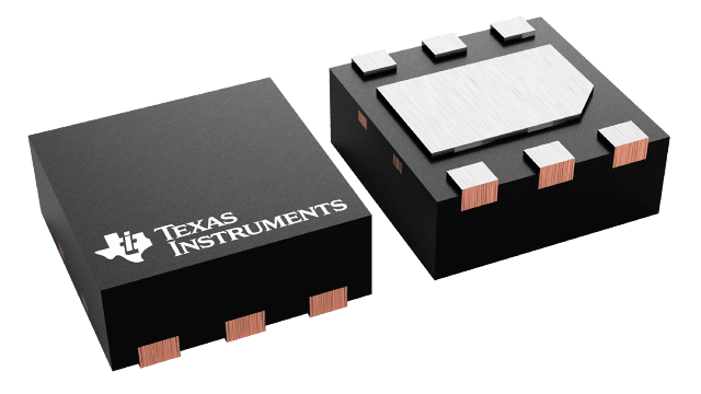
TPS61291DRVR
ActiveLOW IQ BOOST CONVERTER WITH 15NA BYPASS OPERATION
Deep-Dive with AI
Search across all available documentation for this part.

TPS61291DRVR
ActiveLOW IQ BOOST CONVERTER WITH 15NA BYPASS OPERATION
Deep-Dive with AI
Technical Specifications
Parameters and characteristics for this part
| Specification | TPS61291DRVR |
|---|---|
| Function | Step-Up |
| Mounting Type | Surface Mount |
| Number of Outputs | 1 |
| Operating Temperature [Max] | 85 C |
| Operating Temperature [Min] | -40 ¯C |
| Output Configuration | Positive |
| Output Type | Programmable |
| Supplier Device Package | 6-WSON (2x2) |
| Synchronous Rectifier | True |
| Topology | Boost |
| Voltage - Input (Max) [Max] | 5 V |
| Voltage - Input (Min) [Min] | 0.9 V |
| Voltage - Output (Min/Fixed) | 2.5 V, 3.3 V, 3 V |
Pricing
Prices provided here are for design reference only. For realtime values and availability, please visit the distributors directly
| Distributor | Package | Quantity | $ | |
|---|---|---|---|---|
| Digikey | Cut Tape (CT) | 1 | $ 1.60 | |
| 10 | $ 1.44 | |||
| 25 | $ 1.35 | |||
| 100 | $ 1.15 | |||
| 250 | $ 1.08 | |||
| 500 | $ 0.95 | |||
| 1000 | $ 0.78 | |||
| Digi-Reel® | 1 | $ 1.60 | ||
| 10 | $ 1.44 | |||
| 25 | $ 1.35 | |||
| 100 | $ 1.15 | |||
| 250 | $ 1.08 | |||
| 500 | $ 0.95 | |||
| 1000 | $ 0.78 | |||
| N/A | 4758 | $ 1.58 | ||
| Tape & Reel (TR) | 3000 | $ 0.73 | ||
| 6000 | $ 0.70 | |||
| Texas Instruments | LARGE T&R | 1 | $ 1.20 | |
| 100 | $ 0.99 | |||
| 250 | $ 0.71 | |||
| 1000 | $ 0.54 | |||
Description
General part information
TPS61291 Series
The TPS61291 is a boost converter with pin selectable output voltages and an integrated bypass mode. In bypass operation, the device provides a direct path from the input to the system and allows a low power micro controller (MCU) such as the MSP430 to operate directly from a single 3V Li-MnO2 battery or dual alkaline battery cells.
In bypass mode the integrated feedback divider network for boost mode operation is disconnected from the output and the quiescent current consumption drops down to only 15nA (typical).
In boost mode the device provides a minimum output current of 200mA at 3.3V VOUTfrom 1.8V VIN. The boost mode is used for system components which require a regulated supply voltage and cannot directly operate from the input source. The boost converter is based on a current-mode controller using synchronous rectification to obtain maximum efficiency and consumes typically 5.7µA from the output. During startup of the boost converter, the VSEL pin is read out and the integrated feedback network sets the output voltage to 2.5V, 3V or 3.3V.
Documents
Technical documentation and resources


