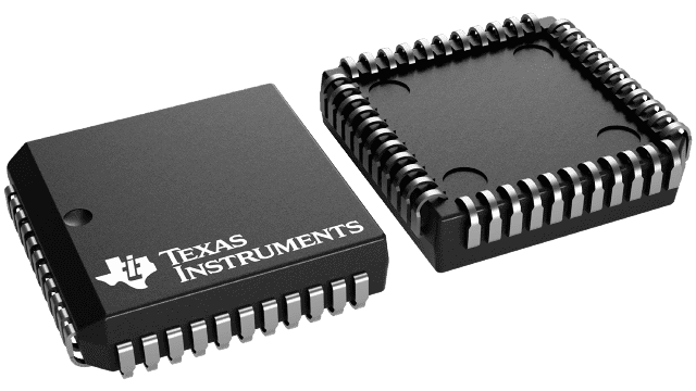
SN74ACT8990FNR
ActiveTEST-BUS CONTROLLERS IEEE STD 1149.1 (JTAG) TAP MASTERS WITH 16-BIT GENERIC HOST INTERFACES
Deep-Dive with AI
Search across all available documentation for this part.

SN74ACT8990FNR
ActiveTEST-BUS CONTROLLERS IEEE STD 1149.1 (JTAG) TAP MASTERS WITH 16-BIT GENERIC HOST INTERFACES
Deep-Dive with AI
Technical Specifications
Parameters and characteristics for this part
| Specification | SN74ACT8990FNR |
|---|---|
| Logic Type | Test Bus Controller |
| Mounting Type | Surface Mount |
| Number of Bits | 16 |
| Operating Temperature [Max] | 70 °C |
| Operating Temperature [Min] | 0 °C |
| Package / Case | 44-LCC (J-Lead) |
| Supplier Device Package | 44-PLCC |
| Supplier Device Package [x] | 16.58 |
| Supplier Device Package [y] | 16.58 |
| Supply Voltage [Max] | 5.5 V |
| Supply Voltage [Min] | 4.5 V |
Pricing
Prices provided here are for design reference only. For realtime values and availability, please visit the distributors directly
| Distributor | Package | Quantity | $ | |
|---|---|---|---|---|
| Digikey | Tape & Reel (TR) | 500 | $ 30.04 | |
| Texas Instruments | LARGE T&R | 1 | $ 39.34 | |
| 100 | $ 34.97 | |||
| 250 | $ 28.75 | |||
| 1000 | $ 25.71 | |||
Description
General part information
SN74ACT8990 Series
The 'ACT8990 test-bus controllers (TBC) are members of the Texas Instruments SCOPETMtestability integrated-circuit family. This family of components supports IEEE Standard 1149.1-1990 (JTAG) boundary scan to facilitate testing of complex circuit-board assemblies. The 'ACT8990 differ from other SCOPETMintegrated circuits. Their function is to control the JTAG serial-test bus rather than being target boundary-scannable devices.
The required signals of the JTAG serial-test bus - test clock (TCK), test mode select (TMS), test data input (TDI), and test data output (TDO) can be connected from the TBC to a target device without additional logic. This is done as a chain of IEEE Standard 1149.1-1990 boundary-scannable components that share the same serial-test bus. The TBC generates TMS and TDI signals for its target(s), receives TDO signals from its target(s), and buffers its test clock input (TCKI) to a test clock output (TCKO) for distribution to its target(s). The TMS, TDI, and TDO signals can be connected to a target directly or via a pipeline, with a retiming delay of up to 31 bits. Since the TBC can be configured to generate up to six separate TMS signals [TMS (5-0)], it can be used to control up to six target scan paths that are connected in parallel (i.e., sharing common TCK, TDI, and TDO signals).
While most operations of the TBC are synchronous to TCKI, a test-off (TOFF\) input is provided for output control of the target interface, and a test-reset (TRST\) input is provided for hardware/software reset of the TBC. In addition, four event [EVENT (3-0)] I/Os are provided for asynchronous communication to target device(s). Each event has its own event generation/detection logic, and detected events can be counted by two 16-bit counters.
Documents
Technical documentation and resources


