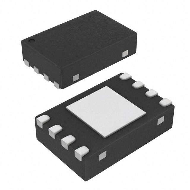
SN65LVP17DRFT
Active2.5-V/3.3-V OSCILLATOR GAIN STAGE/BUFFER WITH ENABLE
Deep-Dive with AI
Search across all available documentation for this part.

SN65LVP17DRFT
Active2.5-V/3.3-V OSCILLATOR GAIN STAGE/BUFFER WITH ENABLE
Deep-Dive with AI
Technical Specifications
Parameters and characteristics for this part
| Specification | SN65LVP17DRFT |
|---|---|
| Current - Supply | 40 mA |
| Data Rate (Max) | 4 Gbps |
| Delay Time | 460 ps |
| Input | PECL |
| Mounting Type | Surface Mount |
| Number of Channels | 1 |
| Operating Temperature [Max] | 85 °C |
| Operating Temperature [Min] | -40 °C |
| Output | LVPECL |
| Package / Case | 8-WFDFN Exposed Pad |
| Supplier Device Package | 8-WSON (2x2) |
| Type | ReDriver, Buffer |
| Voltage - Supply [Max] | 3.6 V |
| Voltage - Supply [Min] | 2.375 V |
Pricing
Prices provided here are for design reference only. For realtime values and availability, please visit the distributors directly
| Distributor | Package | Quantity | $ | |
|---|---|---|---|---|
| Digikey | Cut Tape (CT) | 1 | $ 5.63 | |
| 10 | $ 5.06 | |||
| 25 | $ 4.78 | |||
| 100 | $ 4.14 | |||
| Tape & Reel (TR) | 250 | $ 3.93 | ||
| 500 | $ 3.53 | |||
| 1250 | $ 2.98 | |||
| 2500 | $ 2.83 | |||
| Texas Instruments | SMALL T&R | 1 | $ 3.87 | |
| 100 | $ 3.16 | |||
| 250 | $ 2.48 | |||
| 1000 | $ 2.10 | |||
Description
General part information
SN65LVP17 Series
These four devices are high-frequency oscillator gain stages supporting both LVPECL or LVDS on the high gain outputs in 3.3-V or 2.5-V systems. Additionally, provides the option of both single-ended input (PECL levels on the SN65LVx16) and fully differential inputs on the SN65LVx17.
The SN65LVx16 provides the user a Gain Control (GC) for controlling theQoutput from 300 mV to 860 mV either by leaving it open (NC), grounded, or tied to VCC. (When left open, theQoutput defaults to 575 mV.) TheQon the SN65LVx17 defaults to 575 mV as well.
Both devices provide a voltage reference (VBB) of typically 1.35 V below VCCfor use in receiving single-ended PECL input signals. When not used, VBBshould be unconnected or open.
Documents
Technical documentation and resources


