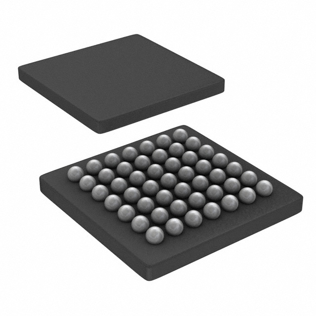
SN65LVDS311YFFT
ActivePROGRAMMABLE 27-BIT DISPLAY SERIAL INTERFACE TRANSMITTER
Deep-Dive with AI
Search across all available documentation for this part.

SN65LVDS311YFFT
ActivePROGRAMMABLE 27-BIT DISPLAY SERIAL INTERFACE TRANSMITTER
Deep-Dive with AI
Technical Specifications
Parameters and characteristics for this part
| Specification | SN65LVDS311YFFT |
|---|---|
| Applications | Cell Phone |
| Interface | Serial |
| Mounting Type | Surface Mount |
| Package / Case | 49-UFBGA, DSBGA |
| Supplier Device Package | 49-DSBGA (2.8x2.8) |
| Voltage - Supply [Max] | 1.95 V |
| Voltage - Supply [Min] | 1.65 V |
Pricing
Prices provided here are for design reference only. For realtime values and availability, please visit the distributors directly
| Distributor | Package | Quantity | $ | |
|---|---|---|---|---|
| Digikey | Cut Tape (CT) | 1 | $ 5.37 | |
| 10 | $ 4.10 | |||
| 25 | $ 3.79 | |||
| 100 | $ 3.44 | |||
| Digi-Reel® | 1 | $ 5.37 | ||
| 10 | $ 4.10 | |||
| 25 | $ 3.79 | |||
| 100 | $ 3.44 | |||
| Tape & Reel (TR) | 250 | $ 3.27 | ||
| 500 | $ 3.17 | |||
| 750 | $ 3.12 | |||
| 1250 | $ 3.07 | |||
| 1750 | $ 3.03 | |||
| 2500 | $ 3.00 | |||
| Texas Instruments | SMALL T&R | 1 | $ 4.08 | |
| 100 | $ 3.33 | |||
| 250 | $ 2.62 | |||
| 1000 | $ 2.22 | |||
Description
General part information
SN65LVDS311 Series
The SN65LVDS311 serializer transmits 27 parallel input data over 1, 2, or 3 serial output links. The device pinout is optimized to interface with the OMAP3630 application processor. The device loads a shift register with the 24 pixel bits and 3 control bits from the parallel CMOS input interface. The data are latched into the device by the pixel clock, PCLK. In addition to the 27 bits, the device adds a parity bit and two reserved bits for a total number of 30 serial bits. The parity bit allows a receiver to detect single-bit errors. Odd parity is implemented.
The serial shift register is uploaded through 1, 2, or 3 serial outputs at 30, 15, or 10 times the pixel clock data rate. A copy of the pixel clock is output on an additional differential output. The serial data and clock are transmitted via Sub Low-Voltage Differential Signaling (SubLVDS) lines. The SN65LVDS311 supports three power modes (Shutdown, Standby and Active) to conserve power.
When transmitting, the PLL locks to the incoming pixel clock PCLK and generates an internal high-speed clock at the line rate of the data lines. The parallel data is latched on the rising edge of PCLK. The serialized data is presented on the serial outputs D0, D1, D2 with a recreation of the Pixel clock PCLK generated from the internal high-speed clock and output on the CLK output. If the input clock PCLK stops, the device enters a standby mode to conserve power.
Documents
Technical documentation and resources


