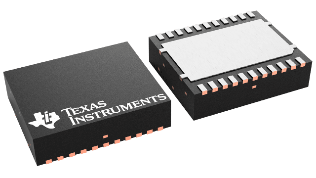
CSD96371Q5M
Active20V 30A SON 5 X 6MM SYNCHRONOUS BUCK NEXFET™ POWER STAGE
Deep-Dive with AI
Search across all available documentation for this part.

CSD96371Q5M
Active20V 30A SON 5 X 6MM SYNCHRONOUS BUCK NEXFET™ POWER STAGE
Deep-Dive with AI
Technical Specifications
Parameters and characteristics for this part
| Specification | CSD96371Q5M |
|---|---|
| Applications | Synchronous Buck Converters |
| Current - Output / Channel | 50 A |
| Current - Peak Output | 75 A |
| Fault Protection | Shoot-Through, UVLO |
| Features | Bootstrap Circuit |
| Interface | PWM |
| Load Type | Inductive |
| Mounting Type | Surface Mount |
| Operating Temperature [Max] | 150 °C |
| Operating Temperature [Min] | -40 °C |
| Package / Case | 22-PowerLFDFN |
| Supplier Device Package | 22-LSON-CLIP (6x5) |
| Technology | Power MOSFET |
| Voltage - Load [Max] | 13.2 V |
| Voltage - Load [Min] | 3.3 V |
| Voltage - Supply [Max] | 5.5 V |
| Voltage - Supply [Min] | 4.5 V |
Pricing
Prices provided here are for design reference only. For realtime values and availability, please visit the distributors directly
| Distributor | Package | Quantity | $ | |
|---|---|---|---|---|
| Digikey | Cut Tape (CT) | 1 | $ 3.37 | |
| Digi-Reel® | 1 | $ 3.37 | ||
| Tape & Reel (TR) | 2500 | $ 1.64 | ||
| 5000 | $ 1.57 | |||
| Texas Instruments | LARGE T&R | 1 | $ 2.54 | |
| 100 | $ 2.23 | |||
| 250 | $ 1.56 | |||
| 1000 | $ 1.26 | |||
Description
General part information
CSD96371Q5M Series
The CSD96371Q5M NexFET Power Stage has an optimized design for use in a high power high density Synchronous Buck converter. This product integrates the gate driver IC and Power MOSFETs to complete the power stage switching function. This combination produces high current, high efficiency, and high speed switching capability in a small 5-mm × 6-mm outline package. In addition, the PCB footprint has been optimized to help reduce design time and simplify the completion of the overall system design.
The CSD96371Q5M NexFET Power Stage has an optimized design for use in a high power high density Synchronous Buck converter. This product integrates the gate driver IC and Power MOSFETs to complete the power stage switching function. This combination produces high current, high efficiency, and high speed switching capability in a small 5-mm × 6-mm outline package. In addition, the PCB footprint has been optimized to help reduce design time and simplify the completion of the overall system design.
Documents
Technical documentation and resources


