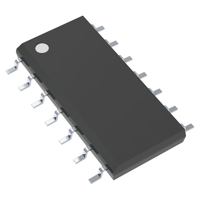
FAN7392MX
Obsolete625V, 3.3/5V INPUT LOGIC COMPATIBLE, 3/3A SINK/SOURCE CURRENT, HIGH & LOW SIDE GATE-DRIVE WITH SD PROTECTION

FAN7392MX
Obsolete625V, 3.3/5V INPUT LOGIC COMPATIBLE, 3/3A SINK/SOURCE CURRENT, HIGH & LOW SIDE GATE-DRIVE WITH SD PROTECTION
Technical Specifications
Parameters and characteristics for this part
| Specification | FAN7392MX |
|---|---|
| Channel Type | Independent |
| Current - Peak Output (Source, Sink) [custom] | 3 A |
| Current - Peak Output (Source, Sink) [custom] | 3 A |
| Driven Configuration | Half-Bridge |
| Gate Type | N-Channel MOSFET, IGBT |
| High Side Voltage - Max (Bootstrap) [Max] | 600 V |
| Input Type | Non-Inverting |
| Logic Voltage - VIL, VIH | 4.5 V, 9.5 V |
| Mounting Type | Surface Mount |
| Number of Drivers | 2 |
| Operating Temperature [Max] | 150 °C |
| Operating Temperature [Min] | -40 °C |
| Package / Case | 16-SOIC |
| Package / Case [x] | 0.295 in |
| Package / Case [y] | 7.5 mm |
| Rise / Fall Time (Typ) [custom] | 20 ns |
| Rise / Fall Time (Typ) [custom] | 25 ns |
| Supplier Device Package | 16-SOIC |
| Voltage - Supply [Max] | 20 V |
| Voltage - Supply [Min] | 10 VDC |
Pricing
Prices provided here are for design reference only. For realtime values and availability, please visit the distributors directly
| Distributor | Package | Quantity | $ | |
|---|---|---|---|---|
Description
General part information
FAN7392 Series
The FAN7392 is a monolithic high- and low-side gate drive IC, that can drive high-speed MOSFETs and IGBTs that operate up to +600V. It has a buffered output stage with all NMOS transistors designed for high pulse current driving capability and minimum cross-conduction. ON Semiconductor’s high-voltage process and common-mode noise canceling techniques provide stable operation of the high-side driver under high dv/dt noise circumstances. An advanced level-shift circuit offers high-side gate driver operation up to VS=-9.8V (typical) for VBS=15V. Logic inputs are compatible with standard CMOS or LSTTL output, down to 3.3V logic. The UVLO circuit prevents malfunction when VCCand VBSare lower than the specified threshold voltage. The high-current and low-output voltage drop feature makes this device suitable for halfand full-bridge inverters, like switching-mode power supply and high-power DC-DC converter applications.
Documents
Technical documentation and resources


