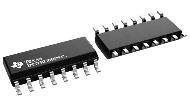
SN74LS221D
ObsoleteDUAL MONOSTABLE MULTIVIBRATORS WITH SCHMITT-TRIGGER INPUTS
Deep-Dive with AI
Search across all available documentation for this part.

SN74LS221D
ObsoleteDUAL MONOSTABLE MULTIVIBRATORS WITH SCHMITT-TRIGGER INPUTS
Technical Specifications
Parameters and characteristics for this part
| Specification | SN74LS221D |
|---|---|
| Current - Output High, Low [custom] | 400 µA |
| Current - Output High, Low [custom] | 8 mA |
| Independent Circuits | 2 |
| Logic Type | Monostable |
| Mounting Type | Surface Mount |
| Operating Temperature [Max] | 70 °C |
| Operating Temperature [Min] | 0 °C |
| Package / Case | 16-SOIC |
| Package / Case [x] | 0.154 in |
| Package / Case [y] | 3.9 mm |
| Propagation Delay | 45 ns |
| Schmitt Trigger Input | False |
| Supplier Device Package | 16-SOIC |
| Voltage - Supply [Max] | 5.25 V |
| Voltage - Supply [Min] | 4.75 V |
Pricing
Prices provided here are for design reference only. For realtime values and availability, please visit the distributors directly
| Distributor | Package | Quantity | $ | |
|---|---|---|---|---|
| Digikey | Tube | 1 | $ 1.66 | |
| 10 | $ 1.48 | |||
| Texas Instruments | TUBE | 1 | $ 1.23 | |
| 100 | $ 0.94 | |||
| 250 | $ 0.69 | |||
| 1000 | $ 0.50 | |||
Description
General part information
SN74LS221 Series
The '221 and 'LS221 devices are monolithic dual multivibrators with performance characteristics virtually identical to those of the '121 devices. Each multivibrator features a negative-transition- triggered input and a positive-transition-triggered input, either of which can be used as an inhibit input.
Pulse triggering occurs at a particular voltage level and is not directly related to the transition time of the input pulse. Schmitt-trigger input circuitry (TTL hysteresis) for B input allows jitter-free triggering from inputs with transition rates as slow as 1 V/s, providing the circuit with excellent noise immunity, typically of 1.2 V. A high immunity to VCCnoise, typically of 1.5 V, is also provided by internal latching circuitry.
Once fired, the outputs are independent of further transitions of the A and B inputs and are a function of the timing components, or the output pulses can be terminated by the overriding clear. Input pulses can be of any duration relative to the output pulse. Output pulse length can be varied from 35 ns to the maximums shown in the above table by choosing appropriate timing components. With Rext= 2 kand Cext= 0, an output pulse typically of 30 ns is achieved, which can be used as a dc-triggered reset signal. Output rise and fall times are TTL compatible and independent of pulse length. Typical triggering and clearing sequences are shown as a part of the switching characteristics waveforms.
Documents
Technical documentation and resources


