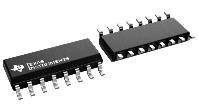
CD74HC670M96
ActiveHIGH SPEED CMOS LOGIC 4-BY-4 REGISTER FILE
Deep-Dive with AI
Search across all available documentation for this part.

CD74HC670M96
ActiveHIGH SPEED CMOS LOGIC 4-BY-4 REGISTER FILE
Deep-Dive with AI
Technical Specifications
Parameters and characteristics for this part
| Specification | CD74HC670M96 |
|---|---|
| Circuit | 1 x 1:1 |
| Independent Circuits | 4 |
| Mounting Type | Surface Mount |
| Operating Temperature [Max] | 125 °C |
| Operating Temperature [Min] | -55 °C |
| Package / Case | 16-SOIC |
| Package / Case [x] | 0.154 in |
| Package / Case [y] | 3.9 mm |
| Supplier Device Package | 16-SOIC |
| Type | Register File |
| Voltage - Supply [Max] | 6 V |
| Voltage - Supply [Min] | 2 V |
| Voltage Supply Source | Single Supply |
CD74HC670 Series
High Speed CMOS Logic 4-by-4 Register File
| Part | Circuit | Independent Circuits | Type | Voltage Supply Source | Supplier Device Package | Mounting Type | Operating Temperature [Min] | Operating Temperature [Max] | Voltage - Supply [Min] | Voltage - Supply [Max] | Package / Case | Package / Case [x] | Package / Case [y] | Package / Case | Package / Case |
|---|---|---|---|---|---|---|---|---|---|---|---|---|---|---|---|
Texas Instruments | 1 x 1:1 | 4 | Register File | Single Supply | 16-SOIC | Surface Mount | -55 °C | 125 °C | 2 V | 6 V | 16-SOIC | 0.154 in | 3.9 mm | ||
Texas Instruments | 1 x 1:1 | 4 | Register File | Single Supply | 16-SOIC | Surface Mount | -55 °C | 125 °C | 2 V | 6 V | 16-SOIC | 0.154 in | 3.9 mm | ||
Texas Instruments | 1 x 1:1 | 4 | Register File | Single Supply | 16-PDIP | Through Hole | -55 °C | 125 °C | 2 V | 6 V | 16-DIP | 0.3 in | 7.62 mm | ||
Texas Instruments | 1 x 1:1 | 4 | Register File | Single Supply | 16-SOIC | Surface Mount | -55 °C | 125 °C | 2 V | 6 V | 16-SOIC | 0.154 in | 3.9 mm |
Pricing
Prices provided here are for design reference only. For realtime values and availability, please visit the distributors directly
| Distributor | Package | Quantity | $ | |
|---|---|---|---|---|
| Digikey | Cut Tape (CT) | 1 | $ 1.52 | |
| 10 | $ 1.36 | |||
| 25 | $ 1.29 | |||
| 100 | $ 1.06 | |||
| 250 | $ 0.99 | |||
| 500 | $ 0.88 | |||
| 1000 | $ 0.69 | |||
| Digi-Reel® | 1 | $ 1.52 | ||
| 10 | $ 1.36 | |||
| 25 | $ 1.29 | |||
| 100 | $ 1.06 | |||
| 250 | $ 0.99 | |||
| 500 | $ 0.88 | |||
| 1000 | $ 0.69 | |||
| Tape & Reel (TR) | 2500 | $ 0.65 | ||
| 5000 | $ 0.61 | |||
| 12500 | $ 0.59 | |||
| Texas Instruments | LARGE T&R | 1 | $ 1.18 | |
| 100 | $ 0.97 | |||
| 250 | $ 0.70 | |||
| 1000 | $ 0.53 | |||
Description
General part information
CD74HC670 Series
The ’HC670 and CD74HCT670 are 16-bit register files organized as 4 words x 4 bits each. Read and write address and enable inputs allow simultaneous writing into one location while reading another. Four data inputs are provided to store the 4-bit word. The write address inputs (WA0 and WA1) determine the location of the stored word in the register. When write enable (WE\) is low the word is entered into the address location and it remains transparent to the data. The outputs will reflect the true form of the input data. When (WE\) is high data and address inputs are inhibited. Data acquisition from the four registers is made possible by the read address inputs (RA1 and RA0). The addressed word appears at the output when the read enable (RE\) is low. The output is in the high impedance state when the (RE\) is high. Outputs can be tied together to increase the word capacity to 512 x 4 bits.
The ’HC670 and CD74HCT670 are 16-bit register files organized as 4 words x 4 bits each. Read and write address and enable inputs allow simultaneous writing into one location while reading another. Four data inputs are provided to store the 4-bit word. The write address inputs (WA0 and WA1) determine the location of the stored word in the register. When write enable (WE\) is low the word is entered into the address location and it remains transparent to the data. The outputs will reflect the true form of the input data. When (WE\) is high data and address inputs are inhibited. Data acquisition from the four registers is made possible by the read address inputs (RA1 and RA0). The addressed word appears at the output when the read enable (RE\) is low. The output is in the high impedance state when the (RE\) is high. Outputs can be tied together to increase the word capacity to 512 x 4 bits.
Documents
Technical documentation and resources


