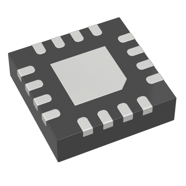
INA851RGTT
ActiveLOW-NOISE (3.2 NV/√HZ) HIGH-SPEED (22 MHZ) FULLY-DIFFERENTIAL INSTRUMENTATION AMP WITH OVP (±40 V)
Deep-Dive with AI
Search across all available documentation for this part.

INA851RGTT
ActiveLOW-NOISE (3.2 NV/√HZ) HIGH-SPEED (22 MHZ) FULLY-DIFFERENTIAL INSTRUMENTATION AMP WITH OVP (±40 V)
Deep-Dive with AI
Technical Specifications
Parameters and characteristics for this part
| Specification | INA851RGTT |
|---|---|
| -3db Bandwidth | 800 kHz |
| Amplifier Type | Instrumentation |
| Current - Input Bias | 5 nA |
| Current - Output / Channel [custom] | 37 mA |
| Current - Supply | 6 mA |
| Mounting Type | Surface Mount |
| Number of Circuits | 1 |
| Operating Temperature [Max] | 125 °C |
| Operating Temperature [Min] | -40 °C |
| Output Type | Differential |
| Package / Case | 16-VFQFN Exposed Pad |
| Slew Rate | 37 V/µs |
| Supplier Device Package | 16-VQFN (3x3) |
| Voltage - Input Offset | 10 µV |
| Voltage - Supply Span (Max) [Max] | 36 V |
| Voltage - Supply Span (Min) [Min] | 8 V |
Pricing
Prices provided here are for design reference only. For realtime values and availability, please visit the distributors directly
| Distributor | Package | Quantity | $ | |
|---|---|---|---|---|
| Digikey | Cut Tape (CT) | 1 | $ 11.51 | |
| 10 | $ 10.40 | |||
| 25 | $ 9.91 | |||
| 100 | $ 8.61 | |||
| Digi-Reel® | 1 | $ 11.51 | ||
| 10 | $ 10.40 | |||
| 25 | $ 9.91 | |||
| 100 | $ 8.61 | |||
| Tape & Reel (TR) | 250 | $ 6.51 | ||
| 500 | $ 5.94 | |||
| 1250 | $ 5.17 | |||
| Texas Instruments | SMALL T&R | 1 | $ 6.98 | |
| 100 | $ 5.69 | |||
| 250 | $ 4.47 | |||
| 1000 | $ 3.79 | |||
Description
General part information
INA851 Series
The INA851 is the industry’s first high-precision instrumentation amplifier with fully differential outputs. This device is optimized to drive inputs of modern high performance analog-to-digital converters (ADCs) with fully differential inputs. The INA851 operates over a very-wide, single-supply or dual-supply range. The output stage gain can be set to either 0.2 or to 1 by shorting or floating two pins. A single external resistor sets any input stage gain from 1 to 10,000.
Compared to other amplifiers in the same class, the INA851 offers very-low input bias current and low input-referred current noise as a result of super-beta input transistors. A state-of-the-art manufacturing process provides exceptionally low voltage noise, input offset voltage, and offset voltage drift. Additional circuitry protects the device inputs against overvoltage up to ±40 V beyond the power-supply voltages.The device outputs feature built-in clamping circuitry to protect the ADC or downstream device against overdrive damage.
The device is designed for operation from either an 8-V minimum single or ±4-V dual supply, and a maximum of 36-V single or ±18 V dual supply.
Documents
Technical documentation and resources


