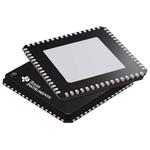
SN65LVDS314RSKR
ActivePROGRAMMABLE 27-BIT SERIAL-TO-PARALLEL RECEIVER
Deep-Dive with AI
Search across all available documentation for this part.

SN65LVDS314RSKR
ActivePROGRAMMABLE 27-BIT SERIAL-TO-PARALLEL RECEIVER
Deep-Dive with AI
Technical Specifications
Parameters and characteristics for this part
| Specification | SN65LVDS314RSKR |
|---|---|
| Data Rate | 1.755 Gbps |
| Mounting Type | Surface Mount |
| Operating Temperature [Max] | 85 °C |
| Operating Temperature [Min] | -40 °C |
| Package / Case | 64-VFQFN Exposed Pad |
| Protocol | LVDS |
| Supplier Device Package | 64-VQFN (8x8) |
| Type | Receiver |
| Voltage - Supply [Max] | 1.95 V |
| Voltage - Supply [Min] | 1.65 V |
Pricing
Prices provided here are for design reference only. For realtime values and availability, please visit the distributors directly
| Distributor | Package | Quantity | $ | |
|---|---|---|---|---|
| Digikey | Cut Tape (CT) | 1 | $ 4.59 | |
| 10 | $ 4.13 | |||
| 25 | $ 3.90 | |||
| 100 | $ 3.38 | |||
| 250 | $ 3.21 | |||
| 500 | $ 2.88 | |||
| 1000 | $ 2.43 | |||
| Digi-Reel® | 1 | $ 4.59 | ||
| 10 | $ 4.13 | |||
| 25 | $ 3.90 | |||
| 100 | $ 3.38 | |||
| 250 | $ 3.21 | |||
| 500 | $ 2.88 | |||
| 1000 | $ 2.43 | |||
| Tape & Reel (TR) | 2000 | $ 2.15 | ||
| Texas Instruments | LARGE T&R | 1 | $ 3.47 | |
| 100 | $ 3.04 | |||
| 250 | $ 2.13 | |||
| 1000 | $ 1.72 | |||
Description
General part information
SN65LVDS314 Series
The SN65LVDS314 receiver de-serializes FlatLink™3G compliant serial input data to 27 parallel data outputs. The SN65LVDS314 receiver contains one shift register to load 30 bits from 1, 2 or 3 serial inputs and latches the 24 pixel bits and 3 control bits out to the parallel CMOS outputs after checking the parity bit. If the parity check confirms correct parity, the Channel Parity Error (CPE) output remains low. If a parity error is detected, the CPE output generates a high pulse while the data output bus disregards the newly-received pixel. Instead, the last data word is held on the output bus for another clock cycle.
The serial data and clock are received via Sub Low-Voltage Differential Signalling (SubLVDS) lines. The SN65LVDS314 supports three operating power modes (Shutdown, Standby, and Active) to conserve power.
When receiving, the PLL locks to the incoming clock CLK and generates an internal high-speed clock at the line rate of the data lines. The data is serially loaded into a shift register using the internal high-speed clock. The deserialized data is presented on the parallel output bus with a recreation of the Pixel clock PCLK generated from the internal high-speed clock. If no input CLK signal is present, the output bus is held static with the PCLK and DE held low, while all other parallel outputs are pulled high.
Documents
Technical documentation and resources


