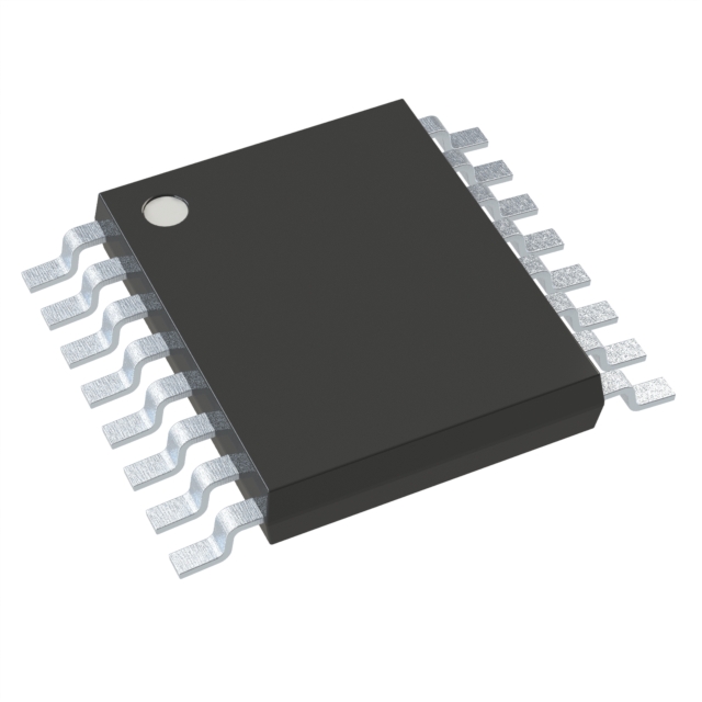
HEF4094BTTJ
ActiveSHIFT REGISTER, HEF4094B, SERIAL TO PARALLEL, SERIAL TO SERIAL, 1 ELEMENT, 8 -BIT, 16 PINS, TSSOP
Deep-Dive with AI
Search across all available documentation for this part.

HEF4094BTTJ
ActiveSHIFT REGISTER, HEF4094B, SERIAL TO PARALLEL, SERIAL TO SERIAL, 1 ELEMENT, 8 -BIT, 16 PINS, TSSOP
Deep-Dive with AI
Technical Specifications
Parameters and characteristics for this part
| Specification | HEF4094BTTJ |
|---|---|
| Function | Serial to Parallel |
| Logic Type | Shift Register |
| Mounting Type | Surface Mount |
| Number of Bits per Element | 8 |
| Number of Elements | 1 |
| Operating Temperature [Max] | 125 °C |
| Operating Temperature [Min] | -40 °C |
| Output Type | Tri-State |
| Package / Case | 16-TSSOP |
| Package / Case [x] | 0.173 in |
| Package / Case [y] | 4.4 mm |
| Supplier Device Package | 16-TSSOP |
| Voltage - Supply [Max] | 15 V |
| Voltage - Supply [Min] | 3 V |
Pricing
Prices provided here are for design reference only. For realtime values and availability, please visit the distributors directly
| Distributor | Package | Quantity | $ | |
|---|---|---|---|---|
| Digikey | Cut Tape (CT) | 1 | $ 0.61 | |
| 10 | $ 0.53 | |||
| 25 | $ 0.50 | |||
| 100 | $ 0.41 | |||
| 250 | $ 0.38 | |||
| 500 | $ 0.32 | |||
| 1000 | $ 0.26 | |||
| Digi-Reel® | 1 | $ 0.61 | ||
| 10 | $ 0.53 | |||
| 25 | $ 0.50 | |||
| 100 | $ 0.41 | |||
| 250 | $ 0.38 | |||
| 500 | $ 0.32 | |||
| 1000 | $ 0.26 | |||
| Tape & Reel (TR) | 2500 | $ 0.22 | ||
| 5000 | $ 0.21 | |||
| 12500 | $ 0.20 | |||
| 25000 | $ 0.19 | |||
Description
General part information
HEF4094 Series
The HEF4094B is an 8-bit serial-in/serial or parallel-out shift register with a storage register and 3-state outputs. Both the shift and storage register have separate clocks. The device features a serial input (D) and two serial outputs (QS1 and QS2) to enable cascading. Data is shifted on the LOW-to-HIGH transitions of the CP input. Data is available at QS1 on the LOW-to-HIGH transitions of the CP input to allow cascading when clock edges are fast. The same data is available at QS2 on the next HIGH-to-LOW transition of the CP input to allow cascading when clock edges are slow. The data in the shift register is transferred to the storage register when the STR input is HIGH. Data in the storage register appears at the outputs whenever the output enable input (OE) is HIGH. A LOW on OE causes the outputs to assume a high-impedance OFF-state. Operation of the OE input does not affect the state of the registers. Inputs include clamp diodes. This enables the use of current limiting resistors to interface inputs to voltages in excess of VDD.
Documents
Technical documentation and resources


