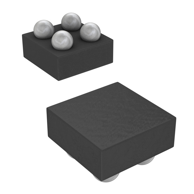
LMV226TL/NOPB
ActiveRF DETECTOR 450MHZ TO 2000MHZ 15DBM 4-PIN DSBGA T/R
Deep-Dive with AI
Search across all available documentation for this part.

LMV226TL/NOPB
ActiveRF DETECTOR 450MHZ TO 2000MHZ 15DBM 4-PIN DSBGA T/R
Technical Specifications
Parameters and characteristics for this part
| Specification | LMV226TL/NOPB |
|---|---|
| Accuracy | 1 dB |
| Current - Supply | 8 mA |
| Frequency [Max] | 2 GHz |
| Frequency [Min] | 450 MHz |
| Input Range [Max] | 15 dBm |
| Input Range [Min] | -15 dBm |
| Mounting Type | Surface Mount |
| Package / Case | DSBGA, 4-WFBGA |
| RF Type | GPRS, EDGE, W-CDMA, TDMA, GSM, Cellular, CDMA2000, CDMA |
| Supplier Device Package | 4-DSBGA (1x1) |
| Voltage - Supply [Max] | 5 V |
| Voltage - Supply [Min] | 2.7 V |
Pricing
Prices provided here are for design reference only. For realtime values and availability, please visit the distributors directly
| Distributor | Package | Quantity | $ | |
|---|---|---|---|---|
| Digikey | Cut Tape (CT) | 1 | $ 1.89 | |
| 10 | $ 1.70 | |||
| 25 | $ 1.60 | |||
| 100 | $ 1.36 | |||
| Digi-Reel® | 1 | $ 1.89 | ||
| 10 | $ 1.70 | |||
| 25 | $ 1.60 | |||
| 100 | $ 1.36 | |||
| Tape & Reel (TR) | 250 | $ 0.87 | ||
| 500 | $ 0.77 | |||
| Texas Instruments | SMALL T&R | 1 | $ 1.42 | |
| 100 | $ 1.17 | |||
| 250 | $ 0.84 | |||
| 1000 | $ 0.63 | |||
Description
General part information
LMV226 Series
The LMV225/LMV226/LMV228 are 30 dB RF power detectors intended for use in CDMA and WCDMA applications. The device has an RF frequency range from 450 MHz to 2 GHz. It provides an accurate temperature and supply compensated output voltage that relates linearly to the RF input power in dBm. The circuit operates with a single supply from 2.7V to 5.5V. The LMV225/LMV226/LMV228 have an integrated filter for low-ripple average power detection of CDMA signals with 30 dB dynamic range. Additional filtering can be applied using a single external capacitor.
The LMV225 has an RF power detection range from –30 dBm to 0 dBm and is ideally suited for direct use in combination with resistive taps. The LMV226/LMV228 have a detection range from –15 dBm to 15 dBm and are intended for use in combination with a directional coupler. The LMV226 is equipped with a buffered output which makes it suitable for GSM, EDGE, GPRS and TDMA applications.
The device is active for Enable = HI, otherwise it is in a low power consumption shutdown mode. During shutdown the output will be LOW. The output voltage ranges from 0.2V to 2V and can be scaled down to meet ADC input range requirements.
Documents
Technical documentation and resources


