5V925BQGI
ObsoletePROGRAMMABLE LVCMOS/LVTTL CLOCK GENERATOR
Deep-Dive with AI
Search across all available documentation for this part.

5V925BQGI
ObsoletePROGRAMMABLE LVCMOS/LVTTL CLOCK GENERATOR
Deep-Dive with AI
Technical Specifications
Parameters and characteristics for this part
| Specification | 5V925BQGI |
|---|---|
| Differential - Input:Output [custom] | False |
| Differential - Input:Output [custom] | False |
| Divider/Multiplier [custom] | False |
| Divider/Multiplier [custom] | False |
| Frequency - Max [Max] | 160 MHz |
| Input | LVTTL, LVCMOS, Crystal |
| Mounting Type | Surface Mount |
| Number of Circuits | 1 |
| Operating Temperature [Max] | 85 °C |
| Operating Temperature [Min] | -40 C |
| Output | LVTTL, LVCMOS |
| Package / Case | 16-SSOP |
| Package / Case [x] | 0.154 in |
| Package / Case [y] | 3.9 mm |
| PLL | True |
| Ratio - Input:Output | 2:4 |
| Supplier Device Package | 16-QSOP |
| Voltage - Supply [Max] | 3.6 V |
| Voltage - Supply [Min] | 3 V |
Pricing
Prices provided here are for design reference only. For realtime values and availability, please visit the distributors directly
| Distributor | Package | Quantity | $ | |
|---|---|---|---|---|
| Digikey | N/A | 5877 | $ 8.47 | |
| Tube | 100 | $ 8.47 | ||
Description
General part information
5V925B Series
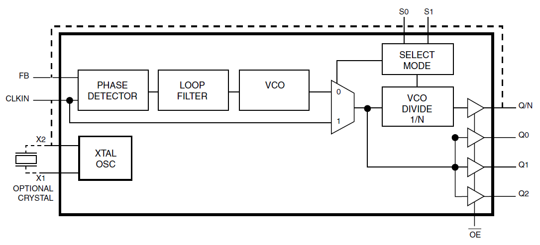
The 5V925BI is a high-performance, low skew, low jitter phase-locked loop (PLL) clock driver. It provides precise phase and frequency alignment of its clock outputs to an externally applied clock input or internal crystal oscillator. The 5V925BI has been specially designed to interface with Gigabit Ethernet and Fast Ethernet applications by providing a 125MHz clock from 25MHz input. It can also be programmed to provide output frequencies ranging from 3.125MHz to 160MHz with input frequencies ranging from 3.125MHz to 80MHz.
Documents
Technical documentation and resources


