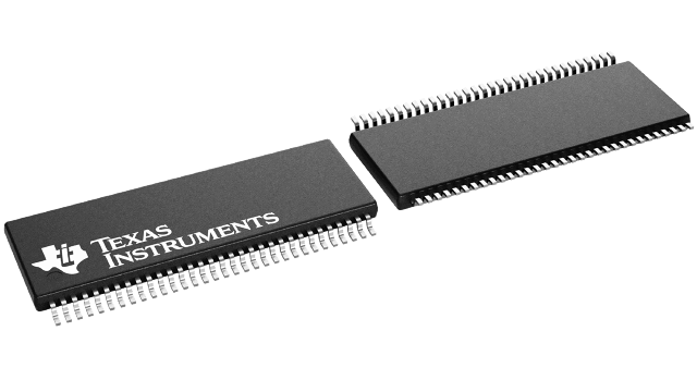
SN74GTL16622ADGGR
Active18-BIT LVTTL TO GTL/GTL+ BUS TRANSCEIVER
Deep-Dive with AI
Search across all available documentation for this part.

SN74GTL16622ADGGR
Active18-BIT LVTTL TO GTL/GTL+ BUS TRANSCEIVER
Technical Specifications
Parameters and characteristics for this part
| Specification | SN74GTL16622ADGGR |
|---|---|
| Channel Type | Bidirectional |
| Channels per Circuit | 9 |
| Input Signal | LVTTL |
| Mounting Type | Surface Mount |
| Number of Circuits | 2 |
| Operating Temperature [Max] | 85 °C |
| Operating Temperature [Min] | -40 °C |
| Output Signal | GTL |
| Output Type | Tri-State, Non-Inverted |
| Package / Case | 6.1 mm |
| Package / Case | 64-TFSOP |
| Package / Case [x] | 0.24 in |
| Supplier Device Package | 64-TSSOP |
| Translator Type | Mixed Signal |
Pricing
Prices provided here are for design reference only. For realtime values and availability, please visit the distributors directly
| Distributor | Package | Quantity | $ | |
|---|---|---|---|---|
| Digikey | Cut Tape (CT) | 1 | $ 15.10 | |
| Digi-Reel® | 1 | $ 15.10 | ||
| Tape & Reel (TR) | 2000 | $ 9.20 | ||
| Texas Instruments | LARGE T&R | 1 | $ 11.82 | |
| 100 | $ 10.32 | |||
| 250 | $ 7.96 | |||
| 1000 | $ 7.12 | |||
Description
General part information
SN74GTL16622A Series
The SN74GTL16622A is an 18-bit registered bus transceiver that provides LVTTL-to-GTL/GTL+ and GTL/GTL+-to-LVTTL signal-level translation. This device is partitioned as two separate 9-bit transceivers with individual clock-enable controls and contains D-type flip-flops for temporary storage of data flowing in either direction. This device provides an interface between cards operating at LVTTL logic levels and a backplane operating at GTL/GTL+ signal levels. Higher speed operation is a direct result of the reduced output swing (<1 V), reduced input threshold levels, and OEC™ circuitry.
The user has the flexibility of using this device at either GTL (VTT= 1.2 V and VREF= 0.8 V) or the preferred higher noise margin GTL+ (VTT= 1.5 V and VREF= 1 V) signal levels. GTL+ is the Texas Instruments derivative of the Gunning Transceiver Logic (GTL) JEDEC standard JESD 8-3. The B port normally operates at GTL or GTL+ signal levels, while the A-port and control inputs are compatible with LVTTL logic levels and are 5-V tolerant. VREFis the reference input voltage for the B port.
Data flow in each direction is controlled by the output-enable (OEAB\ and OEBA\) and clock (CLKAB and CLKBA) inputs. The clock-enable (CEAB\ and CEBA\) inputs control each 9-bit transceiver independently, which makes the device more versatile. For A-to-B data flow, the device operates on the low-to-high transition of CLKAB if CEAB\ is low. When OEAB\ is low, the outputs are active. When OEAB\ is high, the outputs are in the high-impedance state. Data flow for B to A is similar to that of A to B, but uses OEBA\, CLKBA, and CEBA\.
Documents
Technical documentation and resources


