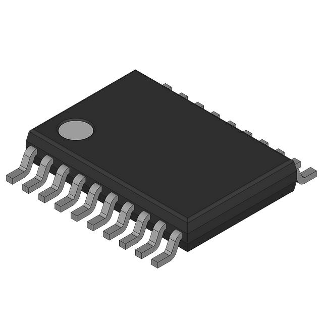
74VHCT574AMTC
ActiveOCTAL D-TYPE FLIP-FLOP WITH 3-STATE OUTPUTS
Deep-Dive with AI
Search across all available documentation for this part.

74VHCT574AMTC
ActiveOCTAL D-TYPE FLIP-FLOP WITH 3-STATE OUTPUTS
Deep-Dive with AI
Technical Specifications
Parameters and characteristics for this part
| Specification | 74VHCT574AMTC |
|---|---|
| Clock Frequency | 130 MHz |
| Current - Output High, Low [custom] | 8 mA |
| Current - Output High, Low [custom] | 8 mA |
| Current - Quiescent (Iq) | 4 çA |
| Function | Standard |
| Input Capacitance | 4 pF |
| Max Propagation Delay @ V, Max CL | 10.4 ns |
| Mounting Type | Surface Mount |
| Number of Bits per Element | 8 |
| Number of Elements | 1 |
| Operating Temperature [Max] | 85 °C |
| Operating Temperature [Min] | -40 °C |
| Output Type | Tri-State, Non-Inverted |
| Package / Case | 20-TSSOP |
| Package / Case [x] | 0.173 in |
| Package / Case [y] | 4.4 mm |
| Supplier Device Package | 20-TSSOP |
| Trigger Type | Positive Edge |
| Type | D-Type |
| Voltage - Supply [Max] | 5.5 V |
| Voltage - Supply [Min] | 4.5 V |
Pricing
Prices provided here are for design reference only. For realtime values and availability, please visit the distributors directly
| Distributor | Package | Quantity | $ | |
|---|---|---|---|---|
| Digikey | Bulk | 895 | $ 0.34 | |
| 895 | $ 0.34 | |||
Description
General part information
MC74VHCT574A Series
The MC74VHCT574A is an advanced high speed CMOS octal flip-flop with 3-state output fabricated with silicon gate CMOS technology. It achieves high speed operation similar to equivalent Bipolar Schottky TTL while maintaining CMOS low power dissipation.This 8-bit D-type flip-flop is controlled by a clock input and an output enable input. When the output enable input is high, the eight outputs are in a high impedance state.The VHCT inputs are compatible with TTL levels. This device can be used as a level converter for interfacing 3.3V to 5.0V, because it has full 5V CMOS level output swings.The VHCT574A input and output (when disabled) structures provide protection when voltages between 0V and 5.5V are applied, regardless of the supply voltage. These input and output structures help prevent device destruction caused by supply voltage - input/output voltage mismatch, battery backup, hot insertion, etc.
Documents
Technical documentation and resources


