Deep-Dive with AI
Search across all available documentation for this part.

Deep-Dive with AI
Technical Specifications
Parameters and characteristics for this part
| Specification | SMJ320C50GFAM66 |
|---|---|
| Clock Rate | 66 MHz |
| Interface | Serial Port |
| Mounting Type | Through Hole |
| On-Chip RAM | 20 kB |
| Operating Temperature [Max] | 125 °C |
| Operating Temperature [Min] | -55 °C |
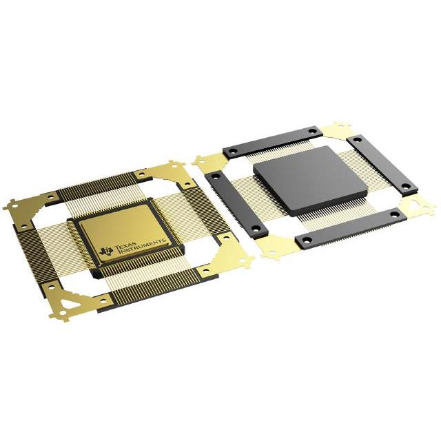
| Package / Case | 141-BCPGA Exposed Pad |
| Supplier Device Package | 141-CPGA |
| Supplier Device Package [x] | 26.92 |
| Supplier Device Package [y] | 26.92 |
| Type | Fixed Point |
| Voltage - Core | 5 V |
| Voltage - I/O | 5 V |
Pricing
Prices provided here are for design reference only. For realtime values and availability, please visit the distributors directly
| Distributor | Package | Quantity | $ | |
|---|---|---|---|---|
| Texas Instruments | JEDEC TRAY (5+1) | 1 | $ 749.64 | |
| 100 | $ 678.56 | |||
| 250 | $ 659.17 | |||
| 1000 | $ 646.25 | |||
Description
General part information
SMJ320C50 Series
The SMJ320C50 digital signal processor (DSP) is a high-performance, 16-bit, fixed-point processor manufactured in 0.72-um double-level metal CMOS technology. The SMJ320C50 is the first DSP from TI designed as a fully static device. Full-static CMOS design contributes to low power consumption while maintaining high performance, making it ideal for applications such as battery-operated communications systems, satellite systems, and advanced control algorithms.
A number of enhancements to the basic SMJ320C2x architecture give the C50 a minimum 2× performance over the previous generation. A four-deep instruction pipeline, that incorporates delayed branching, delayed call to subroutine, and delayed return from subroutine, allows the C50 to perform instructions in fewer cycles. The addition of a parallel logic unit (PLU) gives the C50 a method for manipulating bits in data memory without using the accumulator and ALU. The C50 has additional shifting and scaling capability for proper alignment of multiplicands or storage of values to data memory.
The C50 achieves its low-power consumption through the IDLE2 instruction. IDLE2 removes the functional clock from the internal hardware of the C50, which puts it into a total-sleep mode that uses only 7 uA. A low-logic level on an external interrupt with a duration of at least five clock cycles ends the IDLE2 mode.
Documents
Technical documentation and resources


