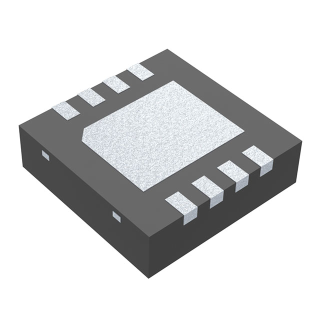
DS25BR120TSD/NOPB
Active3.125-GBPS LVDS BUFFER WITH TRANSMIT PRE-EMPHASIS
Deep-Dive with AI
Search across all available documentation for this part.

DS25BR120TSD/NOPB
Active3.125-GBPS LVDS BUFFER WITH TRANSMIT PRE-EMPHASIS
Technical Specifications
Parameters and characteristics for this part
| Specification | DS25BR120TSD/NOPB |
|---|---|
| Applications | LVDS |
| Current - Supply | 35 mA |
| Delay Time | 350 ps |
| Mounting Type | Surface Mount |
| Number of Channels | 1 |
| Operating Temperature [Max] | 85 °C |
| Operating Temperature [Min] | -40 °C |
| Output | LVDS |
| Package / Case | 8-WFDFN Exposed Pad |
| Signal Conditioning | Output Pre-Emphasis |
| Supplier Device Package | 8-WSON (3x3) |
| Type | ReDriver, Buffer |
| Voltage - Supply [Max] | 3.6 V |
| Voltage - Supply [Min] | 3 V |
Pricing
Prices provided here are for design reference only. For realtime values and availability, please visit the distributors directly
| Distributor | Package | Quantity | $ | |
|---|---|---|---|---|
| Digikey | Cut Tape (CT) | 1 | $ 5.06 | |
| 10 | $ 4.55 | |||
| 25 | $ 4.30 | |||
| 100 | $ 3.73 | |||
| 250 | $ 3.54 | |||
| 500 | $ 3.17 | |||
| Digi-Reel® | 1 | $ 5.06 | ||
| 10 | $ 4.55 | |||
| 25 | $ 4.30 | |||
| 100 | $ 3.73 | |||
| 250 | $ 3.54 | |||
| 500 | $ 3.17 | |||
| Tape & Reel (TR) | 1000 | $ 2.68 | ||
| 2000 | $ 2.54 | |||
| Texas Instruments | SMALL T&R | 1 | $ 3.48 | |
| 100 | $ 2.84 | |||
| 250 | $ 2.23 | |||
| 1000 | $ 1.89 | |||
Description
General part information
DS25BR120 Series
The DS25BR120 is a single channel 3.125 Gbps LVDS buffer optimized for high-speed signal transmission over lossy FR-4 printed circuit board backplanes and balanced metallic cables. Fully differential signal paths ensure exceptional signal integrity and noise immunity.
The DS25BR120 features four levels of pre-emphasis (PE) for use as an optimized driver device. Other LVDS devices with similar IO characteristics include the following products. The DS25BR110 features four levels of equalization for use as an optimized receiver device, while the DS25BR100 features both pre-emphasis and equalization for use as an optimized repeater device. The DS25BR150 is a buffer/repeater with the lowest power consumption and does not feature transmit pre-emphasis nor receive equalization.
Wide input common mode range allows the receiver to accept signals with LVDS, CML and LVPECL levels; the output levels are LVDS. A very small package footprint requires minimal space on the board while the flow-through pinout allows easy board layout. The differential inputs and outputs are internally terminated with a 100Ω resistor to lower device input and output return losses, reduce component count and further minimize board space.
Documents
Technical documentation and resources


