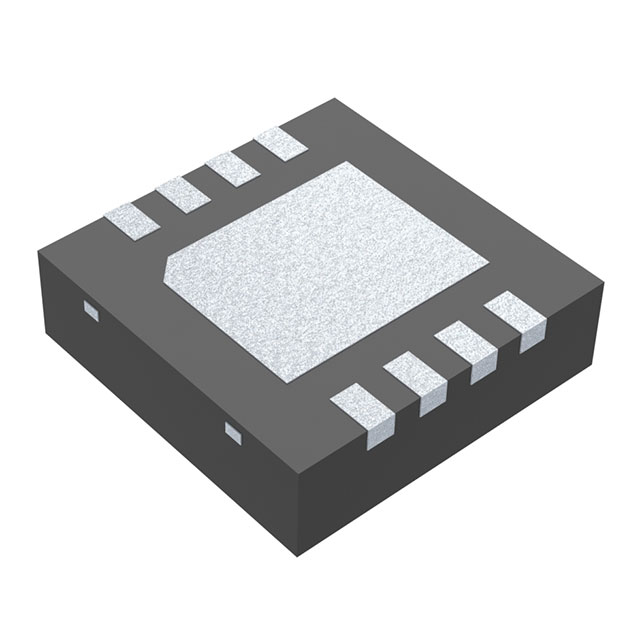
DS25BR110TSD/NOPB
Active3.125-GBPS LVDS BUFFER WITH RECEIVE EQUALIZATION
Deep-Dive with AI
Search across all available documentation for this part.

DS25BR110TSD/NOPB
Active3.125-GBPS LVDS BUFFER WITH RECEIVE EQUALIZATION
Technical Specifications
Parameters and characteristics for this part
| Specification | DS25BR110TSD/NOPB |
|---|---|
| Applications | LVDS |
| Current - Supply | 35 mA |
| Delay Time | 350 ps |
| Input | LVDS |
| Mounting Type | Surface Mount |
| Number of Channels | 1 |
| Operating Temperature [Max] | 85 °C |
| Operating Temperature [Min] | -40 °C |
| Output | LVDS |
| Package / Case | 8-WFDFN Exposed Pad |
| Signal Conditioning | Input Equalization |
| Supplier Device Package | 8-WSON (3x3) |
| Type | ReDriver, Buffer |
| Voltage - Supply [Max] | 3.6 V |
| Voltage - Supply [Min] | 3 V |
Pricing
Prices provided here are for design reference only. For realtime values and availability, please visit the distributors directly
| Distributor | Package | Quantity | $ | |
|---|---|---|---|---|
| Digikey | Cut Tape (CT) | 1 | $ 6.08 | |
| 10 | $ 5.46 | |||
| 25 | $ 5.16 | |||
| 100 | $ 4.47 | |||
| 250 | $ 4.24 | |||
| 500 | $ 3.81 | |||
| Digi-Reel® | 1 | $ 6.08 | ||
| 10 | $ 5.46 | |||
| 25 | $ 5.16 | |||
| 100 | $ 4.47 | |||
| 250 | $ 4.24 | |||
| 500 | $ 3.81 | |||
| Tape & Reel (TR) | 1000 | $ 3.21 | ||
| 2000 | $ 3.05 | |||
| Texas Instruments | SMALL T&R | 1 | $ 4.18 | |
| 100 | $ 3.40 | |||
| 250 | $ 2.68 | |||
| 1000 | $ 2.27 | |||
Description
General part information
DS25BR110 Series
The DS25BR110 is a single channel 3.125 Gbps LVDS buffer optimized for high-speed signal transmission over lossy FR-4 printed circuit board backplanes and balanced metallic cables. A fully differential signal path ensures exceptional signal integrity and noise immunity.
The DS25BR110 features four levels of receive equalization (EQ), making it ideal for use as a receiver device. Other LVDS devices with similar IO characteristics include the following products. The DS25BR120 features four levels of pre-emphasis for use as an optimized driver device, while the DS25BR100 features both pre-emphasis and equalization for use as an optimized repeater device. The DS25BR150 is a buffer/repeater with the lowest power consumption and does not feature transmit pre-emphasis nor receive equalization.
Wide input common mode range allows the receiver to accept signals with LVDS, CML and LVPECL levels; the output levels are LVDS. A very small package footprint requires minimal space on the board while the flow-through pinout allows easy board layout. The differential inputs and outputs are internally terminated with a 100Ω resistor to lower device input and output return losses, reduce component count, and further minimize board space.
Documents
Technical documentation and resources


