9DB106BGILF
Active6-OUTPUT DIFFERENTIAL BUFFER FOR PCIE GEN2
Deep-Dive with AI
Search across all available documentation for this part.

9DB106BGILF
Active6-OUTPUT DIFFERENTIAL BUFFER FOR PCIE GEN2
Deep-Dive with AI
Technical Specifications
Parameters and characteristics for this part
| Specification | 9DB106BGILF |
|---|---|
| Differential - Input:Output [custom] | True |
| Differential - Input:Output [custom] | True |
| Frequency - Max [Max] | 105 MHz |
| Input | Clock |
| Main Purpose | PCI Express (PCIe) |
| Mounting Type | Surface Mount |
| Number of Circuits | 1 |
| Operating Temperature [Max] | 85 °C |
| Operating Temperature [Min] | -40 °C |
| Output | HCSL |
| Package / Case | 28-TSSOP |
| Package / Case | 0.173 in |
| Package / Case [y] | 4.4 mm |
| PLL | True |
| Ratio - Input:Output [custom] | 1:6 |
| Supplier Device Package | 28-TSSOP |
| Voltage - Supply [Max] | 3.465 V |
| Voltage - Supply [Min] | 3.135 V |
Pricing
Prices provided here are for design reference only. For realtime values and availability, please visit the distributors directly
| Distributor | Package | Quantity | $ | |
|---|---|---|---|---|
| Digikey | Tube | 1 | $ 5.73 | |
| 10 | $ 5.14 | |||
| 50 | $ 4.86 | |||
| 100 | $ 4.21 | |||
| 250 | $ 4.00 | |||
| 500 | $ 3.59 | |||
| 1000 | $ 3.03 | |||
| 2500 | $ 2.87 | |||
Description
General part information
9DB106 Series
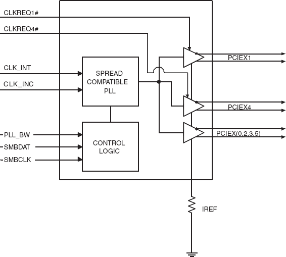
The 9DB106 zero-delay buffer supports PCIe Gen1 and Gen2 clocking requirements. The 9DB106 is driven by a differential SRC output pair from an IDT CK410/CK505-compliant main clock generator. It attenuates jitter on the input clock and has a selectable PLL bandwidth to maximize performance in systems with or without Spread-Spectrum clocking. An SMBus interface allows control of the PLL bandwidth and bypass options, while 2 clock request (CLKREQ#) pins make the 9DB106 suitable for Express Card applications.
Documents
Technical documentation and resources


