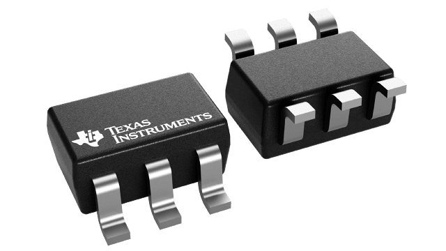
LM66100DCKR
Active1.5-V TO 5.5-V, 1.5-A, 0.5-ΜA IQ IDEAL DIODE WITH INTEGRATED FET
Deep-Dive with AI
Search across all available documentation for this part.

LM66100DCKR
Active1.5-V TO 5.5-V, 1.5-A, 0.5-ΜA IQ IDEAL DIODE WITH INTEGRATED FET
Technical Specifications
Parameters and characteristics for this part
| Specification | LM66100DCKR |
|---|---|
| Applications | General Purpose |
| Current - Output (Max) [Max] | 1.5 A |
| Delay Time - OFF | 2 µs |
| Delay Time - ON | 27 µs |
| FET Type | P-Channel |
| Internal Switch(s) | True |
| Mounting Type | Surface Mount |
| Operating Temperature [Max] | 105 ░C |
| Operating Temperature [Min] | -40 °C |
| Package / Case | 6-TSSOP, SC-88, SOT-363 |
| Ratio - Input:Output [custom] | 1:1 |
| Supplier Device Package | SC-70-6 |
| Voltage - Supply [Max] | 5.5 V |
| Voltage - Supply [Min] | 1.5 V |
Pricing
Prices provided here are for design reference only. For realtime values and availability, please visit the distributors directly
| Distributor | Package | Quantity | $ | |
|---|---|---|---|---|
| Digikey | Cut Tape (CT) | 1 | $ 0.41 | |
| 10 | $ 0.33 | |||
| 25 | $ 0.30 | |||
| 100 | $ 0.23 | |||
| 250 | $ 0.21 | |||
| 500 | $ 0.17 | |||
| 1000 | $ 0.13 | |||
| Digi-Reel® | 1 | $ 0.41 | ||
| 10 | $ 0.33 | |||
| 25 | $ 0.30 | |||
| 100 | $ 0.23 | |||
| 250 | $ 0.21 | |||
| 500 | $ 0.17 | |||
| 1000 | $ 0.13 | |||
| Tape & Reel (TR) | 3000 | $ 0.12 | ||
| 6000 | $ 0.11 | |||
| 15000 | $ 0.10 | |||
| 30000 | $ 0.09 | |||
| 75000 | $ 0.09 | |||
| Texas Instruments | LARGE T&R | 1 | $ 0.20 | |
| 100 | $ 0.14 | |||
| 250 | $ 0.10 | |||
| 1000 | $ 0.07 | |||
Description
General part information
LM66100 Series
The LM66100 is a Single-Input, Single-Output (SISO) integrated ideal diode that is well suited for a variety of applications. The device contains a P-channel MOSFET that can operate over an input voltage range of 1.5 V to 5.5 V and can support a maximum continuous current of 1.5 A.
The chip enable works by comparing theCEpin voltage to the input voltage. When theCEpin voltage is higher than VIN, the device is disabled and the MOSFET is off. When theCEpin voltage is lower, the MOSFET is on. The LM66100 also comes with reverse polarity protection (RPP) that can protect the device from a miswired input, such as a reversed battery.
Two LM66100 devices can be used in an ORing configuration similar to a dual diode ORing implementation. In this configuration, the devices pass the highest input voltage to the output while blocking reverse current flow into the input supplies. These devices can compare input and output voltages to make sure that reverse current is blocked through an internal voltage comparator.
Documents
Technical documentation and resources


