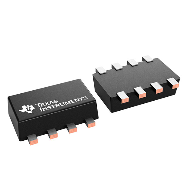
TPS563300DRLR
Active3.8-V TO 28-V INPUT, 3-A SYNCHRONOUS BUCK CONVERTER IN SOT-583 PACKAGE
Deep-Dive with AI
Search across all available documentation for this part.

TPS563300DRLR
Active3.8-V TO 28-V INPUT, 3-A SYNCHRONOUS BUCK CONVERTER IN SOT-583 PACKAGE
Deep-Dive with AI
Technical Specifications
Parameters and characteristics for this part
| Specification | TPS563300DRLR |
|---|---|
| Current - Output | 3 A |
| Frequency - Switching | 500 kHz |
| Function | Step-Down |
| Mounting Type | Surface Mount |
| Number of Outputs | 1 |
| Operating Temperature [Max] | 150 °C |
| Operating Temperature [Min] | -40 °C |
| Output Configuration | Positive |
| Output Type | Adjustable |
| Package / Case | SOT-583 |
| Supplier Device Package | SOT-583 |
| Synchronous Rectifier | True |
| Topology | Buck |
| Voltage - Input (Max) [Max] | 28 V |
| Voltage - Input (Min) [Min] | 3.8 V |
| Voltage - Output (Max) [Max] | 22 V |
| Voltage - Output (Min/Fixed) | 0.8 V |
Pricing
Prices provided here are for design reference only. For realtime values and availability, please visit the distributors directly
| Distributor | Package | Quantity | $ | |
|---|---|---|---|---|
| Digikey | Cut Tape (CT) | 1 | $ 0.83 | |
| 10 | $ 0.74 | |||
| 25 | $ 0.71 | |||
| 100 | $ 0.58 | |||
| 250 | $ 0.54 | |||
| 500 | $ 0.48 | |||
| 1000 | $ 0.38 | |||
| Digi-Reel® | 1 | $ 0.83 | ||
| 10 | $ 0.74 | |||
| 25 | $ 0.71 | |||
| 100 | $ 0.58 | |||
| 250 | $ 0.54 | |||
| 500 | $ 0.48 | |||
| 1000 | $ 0.38 | |||
| Tape & Reel (TR) | 4000 | $ 0.35 | ||
| 8000 | $ 0.34 | |||
| 12000 | $ 0.32 | |||
| 28000 | $ 0.31 | |||
| Texas Instruments | LARGE T&R | 1 | $ 0.74 | |
| 100 | $ 0.57 | |||
| 250 | $ 0.42 | |||
| 1000 | $ 0.30 | |||
Description
General part information
TPS563300 Series
The TPS563300 is a high-efficiency, easy-to-use synchronous buck converter with a wide input voltage range of 3.8 V to 28 V, and supports up to 3-A continuous output current and 0.8-V to 22-V output voltage.
The device employs fixed-frequency peak current control mode for fast transient response and good line and load regulation. The optimized internal loop compensation eliminates external compensation components over a wide range of output voltage and operation frequency. Pulse frequency modulation (PFM) mode maximizes the light load efficiency. The low quiescent current feature is beneficial for long battery life time in low-power operation. The device also has a frequency spread spectrum feature, which helps with lowering down EMI noise.
The device provides complete protections including OTP, OVP, UVLO, cycle-by-cycle OC limit, and UVP with hiccup mode. This device is in a small SOT583 (1.6-mm × 2.1-mm) package with 0.5-mm pin pitch, and has an optimized pinout for easy PCB layout and promotes good EMI performance.
Documents
Technical documentation and resources


