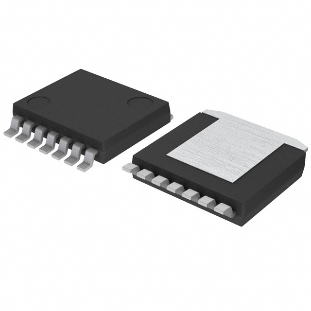
BD90640HFP-CTR
ActiveINPUT 3.5 V TO 36 V OUTPUT 4A 1CH STEP-DOWN REGULATOR
Deep-Dive with AI
Search across all available documentation for this part.

BD90640HFP-CTR
ActiveINPUT 3.5 V TO 36 V OUTPUT 4A 1CH STEP-DOWN REGULATOR
Deep-Dive with AI
Technical Specifications
Parameters and characteristics for this part
| Specification | BD90640HFP-CTR |
|---|---|
| Current - Output | 4 A |
| Frequency - Switching [Max] | 500 kHz |
| Frequency - Switching [Min] | 50 kHz |
| Function | Step-Down |
| Grade | Automotive |
| Mounting Type | Surface Mount |
| Number of Outputs | 1 |
| Operating Temperature [Max] | 125 °C |
| Operating Temperature [Min] | -40 °C |
| Output Configuration | Positive |
| Output Type | Adjustable |
| Package / Case | HRP-7 (7 Leads + Tab) |
| Qualification | AEC-Q100 |
| Supplier Device Package | HRP7 |
| Synchronous Rectifier | False |
| Topology | Buck |
| Voltage - Input (Max) [Max] | 36 V |
| Voltage - Input (Min) [Min] | 5 V |
| Voltage - Output (Max) [Max] | 36 V |
| Voltage - Output (Min/Fixed) | 0.8 V |
Pricing
Prices provided here are for design reference only. For realtime values and availability, please visit the distributors directly
| Distributor | Package | Quantity | $ | |
|---|---|---|---|---|
| Digikey | Cut Tape (CT) | 1 | $ 2.92 | |
| 10 | $ 2.63 | |||
| 25 | $ 2.48 | |||
| 100 | $ 2.11 | |||
| 250 | $ 1.98 | |||
| 500 | $ 1.73 | |||
| 1000 | $ 1.44 | |||
| Digi-Reel® | 1 | $ 2.92 | ||
| 10 | $ 2.63 | |||
| 25 | $ 2.48 | |||
| 100 | $ 2.11 | |||
| 250 | $ 1.98 | |||
| 500 | $ 1.73 | |||
| 1000 | $ 1.44 | |||
| N/A | 6522 | $ 2.59 | ||
| Tape & Reel (TR) | 2000 | $ 1.34 | ||
| 6000 | $ 1.29 | |||
| Newark | Each (Supplied on Cut Tape) | 1 | $ 3.97 | |
| 10 | $ 3.14 | |||
| 25 | $ 2.96 | |||
| 50 | $ 2.78 | |||
| 100 | $ 2.59 | |||
| 300 | $ 2.39 | |||
| 500 | $ 2.31 | |||
| 1000 | $ 2.25 | |||
Description
General part information
BD90640 Series
BD90640UEFJ-C is a step-down switching regulator with integrated POWER MOSFET and have the capability to withstand high input voltage, providing a free setting function of operating switching frequency with external resistor. This switching regulator features a wide input voltage range (3.5V to 36V, Absolute maximum 42V) and operating temperature range (-40℃ to +125℃). Furthermore, an external synchronization input pin enables synchronous operation with external clock.This IC uses different production line against series model BD90640EFJ-C for the purpose of improving production efficiency. We recommend using this IC for your new development. Electric characteristics noted in Datasheet does not differ between Production Line. In addition, the data of BD90640EFJ-C is disclosed for documents and design models unless otherwise specified.
Documents
Technical documentation and resources


