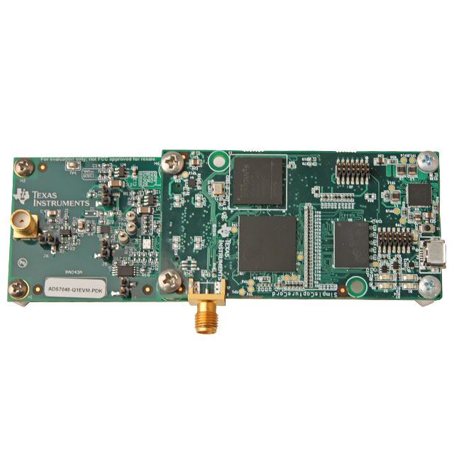
ADS7049-Q1EVM-PDK
ActiveADS7049-Q1 ADC DEMONSTRATION KIT 2MSPS GRAPHICAL USER INTERFACE IDE AUTOMOTIVE AEC-Q100
Deep-Dive with AI
Search across all available documentation for this part.

ADS7049-Q1EVM-PDK
ActiveADS7049-Q1 ADC DEMONSTRATION KIT 2MSPS GRAPHICAL USER INTERFACE IDE AUTOMOTIVE AEC-Q100
Deep-Dive with AI
Technical Specifications
Parameters and characteristics for this part
| Specification | ADS7049-Q1EVM-PDK |
|---|---|
| Data Interface | SPI, Serial |
| Input Range [Max] | Vdd |
| Input Range [Min] | 0 |
| Number of A/D Converters | 1 |
| Number of Bits | 12 bits |
| Power (Typ) @ Conditions | 1.14 mW |
| Sampling Rate (Per Second) | 2M |
| Supplied Contents | Board(s) |
| Utilized IC / Part | ADS7049-Q1 |
Pricing
Prices provided here are for design reference only. For realtime values and availability, please visit the distributors directly
| Distributor | Package | Quantity | $ | |
|---|---|---|---|---|
| Digikey | Bulk | 1 | $ 239.99 | |
Description
General part information
ADS7049-Q1 Series
The ADS7049-Q1 device is a an automotive Q100-qualified, 12-bit, 2-MSPS, analog-to-digital converter (ADC). The device supports a wide analog input voltage range (2.35 V to 3.6 V) and includes a capacitor-based, successive-approximation register (SAR) ADC with an inherent sample-and-hold circuit. The SPI-compatible serial interface is controlled by theCSand SCLK signals. The input signal is sampled with theCSfalling edge and SCLK is used for conversion and serial data output. The device supports a wide digital supply range (1.65 V to 3.6 V), enabling direct interface to a variety of host controllers. The ADS7049-Q1 complies with the JESD8-7A standard for a normal DVDD range (1.65 V to 1.95 V).
The ADS7049-Q1 is available in an 8-pin, miniature, VSSOP package and is specified for operation from –40°C to +125°C. The fast sampling rate of the ADS7049-Q1, along with miniature form-factor and low-power consumption, makes this device suitable for space-constrained and fast-scanning automotive applications.
The ADS7049-Q1 device is a an automotive Q100-qualified, 12-bit, 2-MSPS, analog-to-digital converter (ADC). The device supports a wide analog input voltage range (2.35 V to 3.6 V) and includes a capacitor-based, successive-approximation register (SAR) ADC with an inherent sample-and-hold circuit. The SPI-compatible serial interface is controlled by theCSand SCLK signals. The input signal is sampled with theCSfalling edge and SCLK is used for conversion and serial data output. The device supports a wide digital supply range (1.65 V to 3.6 V), enabling direct interface to a variety of host controllers. The ADS7049-Q1 complies with the JESD8-7A standard for a normal DVDD range (1.65 V to 1.95 V).
Documents
Technical documentation and resources
No documents available


