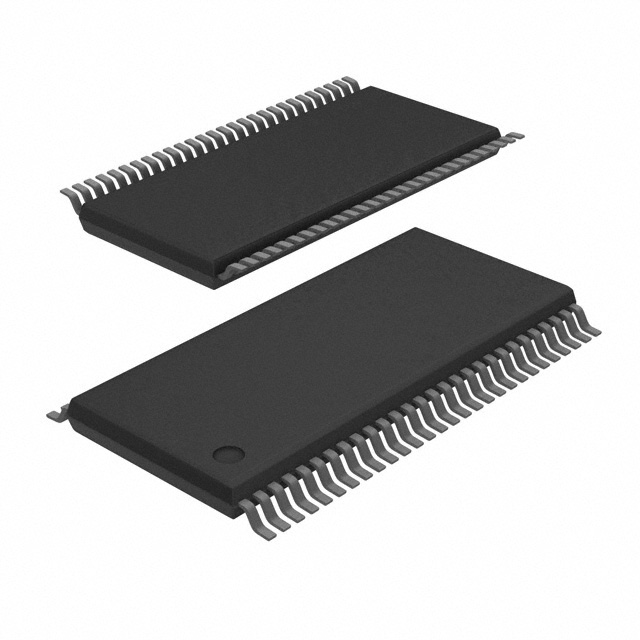
SN74CBTD16211DL
Obsolete5-V, 1:1 (SPST), 24-CHANNEL FET BUS SWITCH WITH LEVEL SHIFTER
Deep-Dive with AI
Search across all available documentation for this part.

SN74CBTD16211DL
Obsolete5-V, 1:1 (SPST), 24-CHANNEL FET BUS SWITCH WITH LEVEL SHIFTER
Deep-Dive with AI
Technical Specifications
Parameters and characteristics for this part
| Specification | SN74CBTD16211DL |
|---|---|
| Circuit [custom] | 1:1 |
| Circuit [custom] | 12 |
| Independent Circuits | 2 |
| Mounting Type | Surface Mount |
| Operating Temperature [Max] | 85 °C |
| Operating Temperature [Min] | -40 °C |
| Package / Case | 0.295 in |
| Package / Case | 56-BSSOP |
| Package / Case | 7.5 mm |
| Supplier Device Package | 56-SSOP |
| Type | Bus Switch |
| Voltage - Supply [Max] | 5.5 V |
| Voltage - Supply [Min] | 4.5 V |
| Voltage Supply Source | Single Supply |
Pricing
Prices provided here are for design reference only. For realtime values and availability, please visit the distributors directly
| Distributor | Package | Quantity | $ | |
|---|---|---|---|---|
| Texas Instruments | TUBE | 1 | $ 2.66 | |
| 100 | $ 2.20 | |||
| 250 | $ 1.58 | |||
| 1000 | $ 1.19 | |||
Description
General part information
SN74CBTD16211 Series
The SN74CBTD16211 provides 24 bits of high-speed TTL-compatible bus switching. The low on-state resistance of the switch allows connections to be made with minimal propagation delay. A diode to VCCis integrated in the circuit to allow for level shifting from 5-V signals at the device inputs to 3.3-V signals at the device outputs.
The device is organized as a dual 12-bit bus switch with separate output-enable (OE)\ inputs. It can be used as two 12-bit bus switches or as one 24-bit bus switch. When (OE)\ is low, the associated 12-bit bus switch is on, and port A is connected to port B. When (OE)\ is high, the switch is open, and the high-impedance state exists between the ports.
The SN74CBTD16211 provides 24 bits of high-speed TTL-compatible bus switching. The low on-state resistance of the switch allows connections to be made with minimal propagation delay. A diode to VCCis integrated in the circuit to allow for level shifting from 5-V signals at the device inputs to 3.3-V signals at the device outputs.
Documents
Technical documentation and resources


