Zenode.ai Logo
Beta
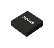
ROHM BD9S231NUX-CE2
Integrated Circuits (ICs)

BD9S231NUX-CE2

Active
Rohm Semiconductor

CONV DC-DC 2.7V TO 5.5V SYNCHRONOUS STEP DOWN SINGLE-OUT 0.8V TO 5.5V 2A 8-PIN VSON-X EP T/R AUTOMOTIVE AEC-Q100

Deep-Dive with AI

Search across all available documentation for this part.

ROHM BD9S231NUX-CE2
Integrated Circuits (ICs)

BD9S231NUX-CE2

Active
Rohm Semiconductor

CONV DC-DC 2.7V TO 5.5V SYNCHRONOUS STEP DOWN SINGLE-OUT 0.8V TO 5.5V 2A 8-PIN VSON-X EP T/R AUTOMOTIVE AEC-Q100

Technical Specifications

Parameters and characteristics for this part

SpecificationBD9S231NUX-CE2
Current - Output2 A
Frequency - Switching2.2 MHz
FunctionStep-Down
GradeAutomotive
Mounting TypeSurface Mount
Number of Outputs1
Operating Temperature [Max]125 °C
Operating Temperature [Min]-40 °C
Output ConfigurationPositive
Output TypeAdjustable
Package / Case8-UFDFN Exposed Pad
QualificationAEC-Q100
Supplier Device PackageVSON008X2020
Synchronous RectifierTrue
TopologyBuck
Voltage - Input (Max) [Max]5.5 V
Voltage - Input (Min) [Min]2.7 V
Voltage - Output (Max) [Max]5.5 V
Voltage - Output (Min/Fixed)0.8 V

Pricing

Prices provided here are for design reference only. For realtime values and availability, please visit the distributors directly

DistributorPackageQuantity$
DigikeyCut Tape (CT) 1$ 1.37
10$ 1.00
25$ 0.90
100$ 0.80
250$ 0.75
500$ 0.72
1000$ 0.70
Digi-Reel® 1$ 1.37
10$ 1.00
25$ 0.90
100$ 0.80
250$ 0.75
500$ 0.72
1000$ 0.70
N/A 3730$ 1.37
Tape & Reel (TR) 4000$ 0.66
8000$ 0.65
12000$ 0.64
NewarkEach (Supplied on Cut Tape) 1$ 2.13
10$ 1.27
25$ 1.13
50$ 1.01
100$ 0.87
250$ 0.83
500$ 0.79
1000$ 0.73

Description

General part information

BD9S231NUX-C Series

BD9S231NUX-C is a synchronous buck DC/DC Converter with built-in low On Resistance power MOSFETs. It is capable of providing current up to 2A. Small inductor is applicable due to high switching frequency of 2.2MHz. It is a current mode control DC/DC Converter and features high-speed transient response. It has a built-in phase compensation circuit. Applications can be created with a few external components.

Documents

Technical documentation and resources

Technical Data Sheet EN

Datasheet

Three Steps for Successful Design of DC-DC Converters

White Paper

Heat Dissipation Effect of Thermal Via in Exposed Pad Type Package

Thermal Design

Power Supply Sequence Circuit with General Purpose Power Supply IC

Schematic Design & Verification

Precautions for PCB Layout Regarding Common Mode Filters

Technical Article

How to Use the Two-Resistor Model

Thermal Design

Impedance Characteristics of Bypass Capacitor

Schematic Design & Verification

What Is Thermal Design

Thermal Design

Solder Joint Rate and Thermal Resistance of Exposed Pad

Thermal Design

Snubber Circuit for Buck Converter IC

Schematic Design & Verification

Factory Information

Manufacturing Data

Considerations for Power Inductors Used for Buck Converters

Schematic Design & Verification

Types of Capacitors Used for Output Smoothing of Switching Regulators and their Precautions

Schematic Design & Verification

Efficiency of Buck Converter

Schematic Design & Verification

PCB Layout Techniques of Buck Converter

Schematic Design & Verification

Judgment Criteria of Thermal Evaluation

Thermal Design

Phase Compensation Design for Current Mode Buck Converter

Schematic Design & Verification

Thermal Resistance

Thermal Design

Overview of ROHM's Simulation Models(for ICs and Discrete Semiconductors)

Technical Article

Five Steps for Successful Thermal Design of IC

White Paper

Diode Selection Method for Asynchronous Converter

Schematic Design & Verification

Method for Determining Constants of Peripheral Parts of Buck DC/DC Converter

Schematic Design & Verification

Step-down DC-DC converter PCB layout EMC Design guide

Schematic Design & Verification

Calculation of Power Loss (Synchronous)

Schematic Design & Verification

PCB Layout Essential Check sheet for Switching Regulator

Schematic Design & Verification

θ<sub>JC</sub> and Ψ<sub>JT</sub>

Thermal Design

Design Guide and Example of Stencil for Exposed Pad

Thermal Design

How to Use the Thermal Resistance and Thermal Characteristics Parameters

Thermal Design

The Important Points of Multi-layer Ceramic Capacitor Used in Buck Converter circuit

Schematic Design & Verification

θ<sub>JA</sub> and Ψ<sub>JT</sub>

Thermal Design

Capacitor Calculation for Buck converter IC

Schematic Design & Verification

Considering Polarity of Power Inductor to Reduce Radiated Emission of DC-DC converter

Schematic Design & Verification

Considering Input Filter to Reduce Conducted Emissions by DCDC Converter

Schematic Design & Verification

Evaluation Board User's Guide for BD9S231NUX-TSB-001

User's Guide

Suppression Method of Switching Noise Using Linear Regulator and Low Pass Filter

Schematic Design & Verification

Method for Calculating Junction Temperature from Transient Thermal Resistance Data

Thermal Design

Precautions When Measuring the Rear of the Package with a Thermocouple

Thermal Design

Calculation of Power Dissipation in Switching Circuit

Schematic Design & Verification

Two-Resistor Model for Thermal Simulation

Thermal Design

Measurement Method for Phase Margin with Frequency Response Analyzer (FRA)

Schematic Design & Verification

PCB Layout Thermal Design Guide

Thermal Design

VSON008X2020 Package Information

Package Information

Bootstrap Circuit in the Buck Converter

Schematic Design & Verification

Cutting-Edge Web Simulation Tool "ROHM Solution Simulator" Capable of Complete Circuit Verification of Power Devices and Driver ICs

White Paper

Resistor Value Table to set Output Voltage of Buck Converter IC

Schematic Design & Verification

Basics of Thermal Resistance and Heat Dissipation

Thermal Design

Inductor Calculation for Buck converter IC

Schematic Design & Verification