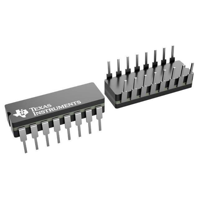
CD54HC194F3A
ActiveHIGH SPEED CMOS LOGIC 4-BIT BIDIRECTIONAL UNIVERSAL SHIFT REGISTER
Deep-Dive with AI
Search across all available documentation for this part.

CD54HC194F3A
ActiveHIGH SPEED CMOS LOGIC 4-BIT BIDIRECTIONAL UNIVERSAL SHIFT REGISTER
Deep-Dive with AI
Technical Specifications
Parameters and characteristics for this part
| Specification | CD54HC194F3A |
|---|---|
| Function | Universal |
| Logic Type | Register, Bidirectional |
| Mounting Type | Through Hole |
| Number of Bits per Element | 4 |
| Number of Elements | 1 |
| Operating Temperature [Max] | 125 °C |
| Operating Temperature [Min] | -55 °C |
| Output Type | Push-Pull |
| Package / Case | 7.62 mm, 0.3 in |
| Package / Case | 16-CDIP |
| Supplier Device Package | 16-CDIP |
| Voltage - Supply [Max] | 6 V |
| Voltage - Supply [Min] | 2 V |
Pricing
Prices provided here are for design reference only. For realtime values and availability, please visit the distributors directly
| Distributor | Package | Quantity | $ | |
|---|---|---|---|---|
| Texas Instruments | TUBE | 1 | $ 26.90 | |
| 100 | $ 23.91 | |||
| 250 | $ 19.66 | |||
| 1000 | $ 17.58 | |||
Description
General part information
CD54HC194 Series
The ’HC194 and CD74HCT194 are 4-bit shift registers with Asynchronous Master Reset (MR)\. In the parallel mode (S0 and S1 are high), data is loaded into the associated flip-flop and appears at the output after the positive transition of the clock input (CP). During parallel loading serial data flow is inhibited. Shift left and shift right are accomplished synchronously on the positive clock edge with serial data entered at the shift left (DSL) serial input for the shift right mode, and at the shift right (DSR) serial input for the shift left mode. Clearing the register is accomplished by a Low applied to the Master Reset (MR)\ pin.
The ’HC194 and CD74HCT194 are 4-bit shift registers with Asynchronous Master Reset (MR)\. In the parallel mode (S0 and S1 are high), data is loaded into the associated flip-flop and appears at the output after the positive transition of the clock input (CP). During parallel loading serial data flow is inhibited. Shift left and shift right are accomplished synchronously on the positive clock edge with serial data entered at the shift left (DSL) serial input for the shift right mode, and at the shift right (DSR) serial input for the shift left mode. Clearing the register is accomplished by a Low applied to the Master Reset (MR)\ pin.
Documents
Technical documentation and resources


