ISL28617FVZ-T7
Obsolete40V PRECISION INSTRUMENTATION AMPLIFIER WITH DIFFERENTIAL ADC DRIVER
Deep-Dive with AI
Search across all available documentation for this part.

ISL28617FVZ-T7
Obsolete40V PRECISION INSTRUMENTATION AMPLIFIER WITH DIFFERENTIAL ADC DRIVER
Deep-Dive with AI
Technical Specifications
Parameters and characteristics for this part
| Specification | ISL28617FVZ-T7 |
|---|---|
| -3db Bandwidth | 5.5 MHz |
| Amplifier Type | Instrumentation |
| Current - Input Bias | 200 pA |
| Current - Output / Channel | 45 mA |
| Mounting Type | Surface Mount |
| Number of Circuits | 1 |
| Operating Temperature [Max] | 125 °C |
| Operating Temperature [Min] | -40 °C |
| Output Type | Differential, Rail-to-Rail |
| Package / Case | 24-TSSOP |
| Package / Case | 0.173 in, 4.4 mm |
| Slew Rate | 4 V/µs |
| Supplier Device Package | 24-TSSOP |
| Voltage - Input Offset | 30 çV |
| Voltage - Supply Span (Max) [Max] | 40 V |
| Voltage - Supply Span (Min) [Min] | 8 V |
Pricing
Prices provided here are for design reference only. For realtime values and availability, please visit the distributors directly
| Distributor | Package | Quantity | $ | |
|---|---|---|---|---|
Description
General part information
ISL28617 Series
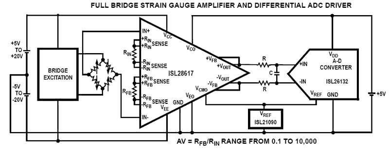
The ISL28617 is a high performance, differential input, differential output instrumentation amplifier designed for precision analog-to-digital applications. It can operate over a supply range of 8V (±4V) to 40V (±20V) and features a differential input voltage range up to ±34V. The output stage has rail-to-rail output drive capability optimized for differential ADC driver applications. Its versatility and small package makes it suitable for a variety of general purpose applications. Additional features not found in other instrumentation amplifiers enable high levels of DC precision and excellent AC performance. The gain of the ISL28617 can be programmed from 0.1 to 10,000 via two external resistors, RINand RFB. The gain accuracy is determined by the matching of RINand RFB. The gain resistors have Kelvin sensing, which removes gain error due to PC trace resistance. The input and output stages have individual power supply pins, which enable input signals riding on a high common mode voltage to be level shifted to a low voltage device, such as an A/D converter. The rail-to-rail output stage can be powered from the same supplies as the ADC, which preserves the ADC maximum input dynamic range and eliminates ADC input overdrive.
Documents
Technical documentation and resources


