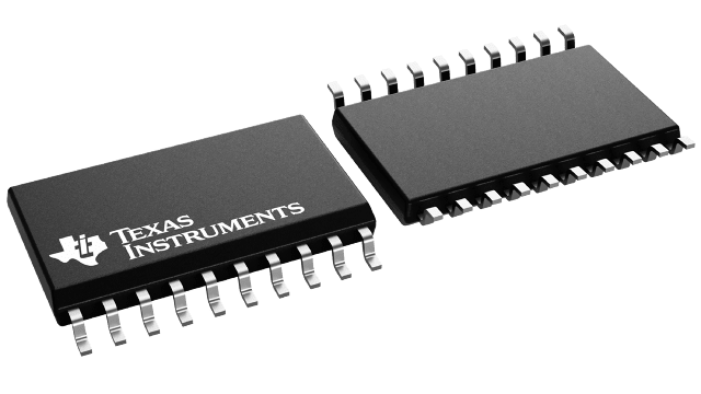
TPIC6B259DWRG4
Unknown8-BIT ADDRESSABLE LATCH WITH 150MA/CH
Deep-Dive with AI
Search across all available documentation for this part.

TPIC6B259DWRG4
Unknown8-BIT ADDRESSABLE LATCH WITH 150MA/CH
Deep-Dive with AI
Technical Specifications
Parameters and characteristics for this part
| Specification | TPIC6B259DWRG4 |
|---|---|
| Circuit | 1:8 |
| Delay Time - Propagation | 150 ns |
| Independent Circuits | 1 |
| Logic Type | D-Type, Addressable |
| Mounting Type | Surface Mount |
| Operating Temperature [Max] | 125 °C |
| Operating Temperature [Min] | -40 °C |
| Output Type | DMOS |
| Package / Case | 20-SOIC |
| Package / Case [y] | 0.295 in |
| Package / Case [y] | 7.5 mm |
| Supplier Device Package | 20-SOIC |
| Voltage - Supply [Max] | 5.5 V |
| Voltage - Supply [Min] | 4.5 V |
Pricing
Prices provided here are for design reference only. For realtime values and availability, please visit the distributors directly
| Distributor | Package | Quantity | $ | |
|---|---|---|---|---|
| Digikey | Tape & Reel (TR) | 2000 | $ 1.07 | |
| 6000 | $ 1.03 | |||
| 10000 | $ 0.99 | |||
| Texas Instruments | LARGE T&R | 1 | $ 1.93 | |
| 100 | $ 1.59 | |||
| 250 | $ 1.14 | |||
| 1000 | $ 0.86 | |||
Description
General part information
TPIC6B259 Series
This power logic 8-bit addressable latch controls open-drain DMOS-transistor outputs and is designed for general-purpose storage applications in digital systems. Specific uses include working registers, serial-holding registers, and decoders or demultiplexers. This is a multi-functional device capable of storing single-line data in eight addressable latches and 3-to-8 decoder or demultiplexer with active-low DMOS outputs.
Four distinct modes of operation are selectable by controlling the clear (CLR\) and enable (G\) inputs as enumerated in the function table. In the addressable-latch mode, data at the data-in (D) terminal is written into the addressed latch. The addressed DMOS-transistor output inverts the data input with all unaddressed DMOS-transistor outputs remaining in their previous states. In the memory mode, all DMOS-transistor outputs remain in their previous states and are unaffected by the data or address inputs. To eliminate the possibility of entering erroneous data in the latch, enable G\ should be held high (inactive) while the address lines are changing. In the 3-to-8 decoding or demultiplexing mode, the addressed output is inverted with respect to the D input and all other
outputs are off. In the clear mode, all outputs are off and unaffected by the address and data inputs. When data is low for a given output, the DMOS-transistor output is off. When data is high, the DMOS-transistor output has sink-current capability.
Documents
Technical documentation and resources


