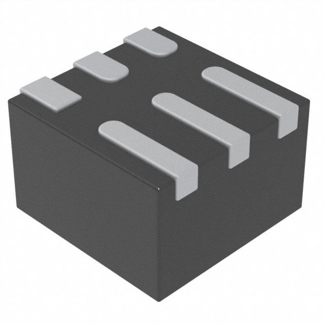
TLV62595DMQR
Active2.5-V TO 5.5-V INPUT, 4-A STEP-DOWN CONVERTER WITH 1% OUTPUT ACCURACY IN 1.5-MM X 1.5-MM QFN PACKAGE
Deep-Dive with AI
Search across all available documentation for this part.

TLV62595DMQR
Active2.5-V TO 5.5-V INPUT, 4-A STEP-DOWN CONVERTER WITH 1% OUTPUT ACCURACY IN 1.5-MM X 1.5-MM QFN PACKAGE
Technical Specifications
Parameters and characteristics for this part
| Specification | TLV62595DMQR |
|---|---|
| Current - Output | 4 A |
| Frequency - Switching | 2.2 MHz |
| Function | Step-Down |
| Mounting Type | Surface Mount |
| Number of Outputs | 1 |
| Operating Temperature [Max] | 125 ¯C |
| Operating Temperature [Min] | -40 °C |
| Output Configuration | Positive |
| Output Type | Adjustable |
| Package / Case | 6-VFDFN |
| Supplier Device Package | 6-VSON-HR (1.5x1.5) |
| Synchronous Rectifier | True |
| Topology | Buck |
| Voltage - Input (Max) [Max] | 5.5 V |
| Voltage - Input (Min) [Min] | 2.5 V |
| Voltage - Output (Max) [Max] | 4 V |
| Voltage - Output (Min/Fixed) | 0.6 V |
Pricing
Prices provided here are for design reference only. For realtime values and availability, please visit the distributors directly
| Distributor | Package | Quantity | $ | |
|---|---|---|---|---|
| Digikey | Cut Tape (CT) | 1 | $ 0.87 | |
| 10 | $ 0.77 | |||
| 25 | $ 0.72 | |||
| 100 | $ 0.59 | |||
| 250 | $ 0.55 | |||
| 500 | $ 0.46 | |||
| 1000 | $ 0.37 | |||
| Digi-Reel® | 1 | $ 0.87 | ||
| 10 | $ 0.77 | |||
| 25 | $ 0.72 | |||
| 100 | $ 0.59 | |||
| 250 | $ 0.55 | |||
| 500 | $ 0.46 | |||
| 1000 | $ 0.37 | |||
| Tape & Reel (TR) | 3000 | $ 0.34 | ||
| 6000 | $ 0.31 | |||
| 15000 | $ 0.30 | |||
| 30000 | $ 0.29 | |||
| Texas Instruments | LARGE T&R | 1 | $ 0.66 | |
| 100 | $ 0.45 | |||
| 250 | $ 0.35 | |||
| 1000 | $ 0.23 | |||
Description
General part information
TLV62595 Series
The TLV62595 is a high-frequency synchronous step-down converter optimized for compact solution size and high efficiency. The device integrates switches capable of delivering an output current up to 4 A. At medium to heavy loads, the converter operates in pulse width modulation (PWM) mode with typical 2.2-MHz switching frequency. At light load, the device automatically enters Power Save Mode (PSM) to maintain high efficiency over the entire load current range with a quiescent current as low as 10 µA.
Based on the DCS Control topology, the device provides a fast transient response. The internal reference regulates the output voltage down to 0.6 V with a high feedback voltage accuracy of 1% over the junction temperature range of –40°C to 125°C. The entire solution requires a small 470-nH inductor, a single 4.7-µF input capacitor and three 10-µF or single 47-µF output capacitor.
The device is available in a 6-pin 1.5-mm × 1.5-mm QFN package, offering a high power density solution.


