MC100ES6130EJ
Obsolete2.5V/3.3V,1:4 PECL CLOCK DRIVER WITH 2:1 INPUT MUX
Deep-Dive with AI
Search across all available documentation for this part.

MC100ES6130EJ
Obsolete2.5V/3.3V,1:4 PECL CLOCK DRIVER WITH 2:1 INPUT MUX
Deep-Dive with AI
Technical Specifications
Parameters and characteristics for this part
| Specification | MC100ES6130EJ |
|---|---|
| Differential - Input:Output [custom] | True |
| Differential - Input:Output [custom] | True |
| Frequency - Max [Max] | 2 GHz |
| Input | LVPECL, HSTL |
| Mounting Type | Surface Mount |
| Number of Circuits | 1 |
| Operating Temperature [Max] | 85 °C |
| Operating Temperature [Min] | -40 °C |
| Output | LVPECL |
| Package / Case | 16-TSSOP |
| Package / Case [x] | 0.173 in |
| Package / Case [y] | 4.4 mm |
| Ratio - Input:Output [custom] | 2:4 |
| Supplier Device Package | 16-TSSOP |
| Type | Fanout Buffer (Distribution), Multiplexer |
| Voltage - Supply [Max] | 3.8 V |
| Voltage - Supply [Min] | 2.375 V |
Pricing
Prices provided here are for design reference only. For realtime values and availability, please visit the distributors directly
| Distributor | Package | Quantity | $ | |
|---|---|---|---|---|
Description
General part information
MC100ES6130 Series
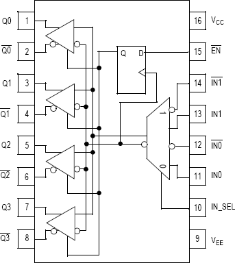
The MC100ES6130 is a 2.5 GHz differential PECL 1:4 fanout buffer. The ES6130 offers a wide operating range of 2.5 V and 3.3 V and also features a 2:1 input MUX which is ideal for redundant clock switchover applications. This device also includes a synchronous enable pin that forces the outputs into a fixed logic state. Enable or disable state is initiated only after the outputs are in a LOW state to eliminate the possibility of a runt clock pulse.
Documents
Technical documentation and resources


