QS3VH257S1G8
Obsolete3.3V QUAD 2:1 MUX/DEMUX FOR HOT SWAP APPLICATIONS
Deep-Dive with AI
Search across all available documentation for this part.

QS3VH257S1G8
Obsolete3.3V QUAD 2:1 MUX/DEMUX FOR HOT SWAP APPLICATIONS
Deep-Dive with AI
Technical Specifications
Parameters and characteristics for this part
| Specification | QS3VH257S1G8 |
|---|---|
| Circuit | 4 x 2:1 |
| Independent Circuits | 1 |
| Mounting Type | Surface Mount |
| Operating Temperature [Max] | 85 °C |
| Operating Temperature [Min] | -40 C |
| Package / Case | 16-SOIC |
| Package / Case | 0.154 in, 3.9 mm |
| Supplier Device Package | 16-SOIC |
| Type | Bus Switch |
| Voltage - Supply [Max] | 3.6 V |
| Voltage - Supply [Min] | 2.3 V |
| Voltage Supply Source | Single Supply |
Pricing
Prices provided here are for design reference only. For realtime values and availability, please visit the distributors directly
| Distributor | Package | Quantity | $ | |
|---|---|---|---|---|
| Digikey | N/A | 1134 | $ 1.84 | |
Description
General part information
QS3VH257 Series
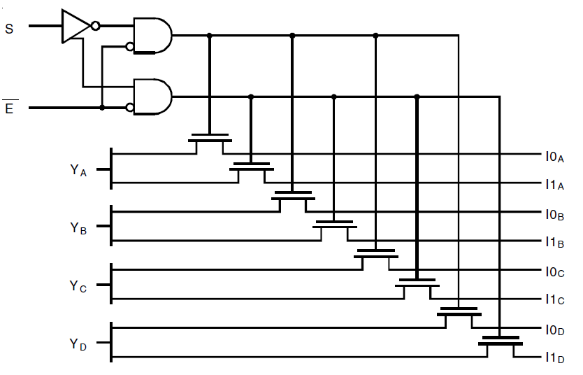
The QS3VH257 HotSwitch quad 2:1 multiplexer/demultiplexer is a high bandwidth bus switch with very low ON-resistance, resulting in under 250ps propagation delay through the switch. The combination of near-zero propagation delay, high OFF impedance, and overvoltage tolerance makes the QS3VH257 ideal for high-performance communication applications. The QS3VH257 operates from -40 °C to +85 °C.
Documents
Technical documentation and resources


