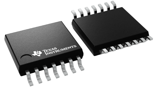
CDCE813R02TPWRQ1
ActivePROGRAMMABLE 1-PLL CLOCK SYNTHESIZER AND JITTER CLEANER WITH 2.5-V AND 3.3-V OUTPUTS
Deep-Dive with AI
Search across all available documentation for this part.

CDCE813R02TPWRQ1
ActivePROGRAMMABLE 1-PLL CLOCK SYNTHESIZER AND JITTER CLEANER WITH 2.5-V AND 3.3-V OUTPUTS
Technical Specifications
Parameters and characteristics for this part
| Specification | CDCE813R02TPWRQ1 |
|---|---|
| Differential - Input:Output | False |
| Frequency - Max [Max] | 230 MHz |
| Grade | Automotive |
| Input | Crystal |
| Mounting Type | Surface Mount |
| Number of Circuits | 1 |
| Operating Temperature [Max] | 105 °C |
| Operating Temperature [Min] | -40 °C |
| Output | LVCMOS |
| Package / Case | 14-TSSOP |
| Package / Case [custom] | 0.173 " |
| Package / Case [custom] | 4.4 mm |
| PLL | Yes with Bypass |
| Qualification | AEC-Q100 |
| Ratio - Input:Output [custom] | 1:3 |
| Supplier Device Package | 14-TSSOP |
| Type | Clock Synthesizer, Jitter Cleaner |
| Voltage - Supply [Max] | 1.9 V |
| Voltage - Supply [Min] | 1.7 V |
Pricing
Prices provided here are for design reference only. For realtime values and availability, please visit the distributors directly
| Distributor | Package | Quantity | $ | |
|---|---|---|---|---|
| Digikey | Cut Tape (CT) | 1 | $ 4.69 | |
| 10 | $ 4.21 | |||
| 25 | $ 3.98 | |||
| 100 | $ 3.45 | |||
| 250 | $ 3.27 | |||
| 500 | $ 2.94 | |||
| 1000 | $ 2.48 | |||
| Digi-Reel® | 1 | $ 4.69 | ||
| 10 | $ 4.21 | |||
| 25 | $ 3.98 | |||
| 100 | $ 3.45 | |||
| 250 | $ 3.27 | |||
| 500 | $ 2.94 | |||
| 1000 | $ 2.48 | |||
| Tape & Reel (TR) | 2000 | $ 2.35 | ||
| Texas Instruments | LARGE T&R | 1 | $ 3.54 | |
| 100 | $ 3.10 | |||
| 250 | $ 2.17 | |||
| 1000 | $ 1.75 | |||
Description
General part information
CDCE813-Q1 Series
The CDCE813-Q1 device is a modular Phase-locked-loop-based (PLL), low-cost, high-performance, programmable clock synthesizers. They generate up to three output clocks from a single input frequency. Each output can be programmed in-system for any clock frequency up to 230MHz, using the integrated configurable PLL.
The CDCE813-Q1 has separate output supply pins, VDDOUT, providing 2.5V to 3.3V.
The input accepts an external crystal or LVCMOS clock signal. A selectable on-chip VCXO allows synchronization of the output frequency to an external control signal.
Documents
Technical documentation and resources


