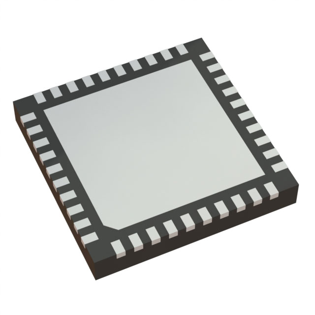
8T49N205A-999NLGI
ObsoleteFEMTOCLOCK NG UNIVERSAL FREQUENCYTRANSLATOR WITH PHASE BUILD-OUT
Deep-Dive with AI
Search across all available documentation for this part.

8T49N205A-999NLGI
ObsoleteFEMTOCLOCK NG UNIVERSAL FREQUENCYTRANSLATOR WITH PHASE BUILD-OUT
Deep-Dive with AI
Technical Specifications
Parameters and characteristics for this part
| Specification | 8T49N205A-999NLGI |
|---|---|
| Differential - Input:Output [custom] | True |
| Differential - Input:Output [custom] | True |
| Divider/Multiplier | Yes/No |
| Frequency - Max [Max] | 1.3 GHz |
| Input | LVDS, Crystal, LVPECL, LVHSTL, HCSL |
| Mounting Type | Surface Mount |
| Number of Circuits | 1 |
| Operating Temperature [Max] | 85 °C |
| Operating Temperature [Min] | -40 °C |
| Output | LVPECL, LVDS |
| Package / Case | 40-VFQFN Exposed Pad |
| PLL | Yes with Bypass |
| Ratio - Input:Output [custom] | 2:2 |
| Supplier Device Package | 40-VFQFPN (6x6) |
| Type | Frequency Translator |
| Voltage - Supply [Max] | 3.465 V |
| Voltage - Supply [Min] | 2.375 V |
Pricing
Prices provided here are for design reference only. For realtime values and availability, please visit the distributors directly
| Distributor | Package | Quantity | $ | |
|---|---|---|---|---|
| Digikey | Tray | 1 | $ 32.73 | |
| 10 | $ 26.53 | |||
| 25 | $ 24.98 | |||
| 80 | $ 23.51 | |||
| 230 | $ 22.53 | |||
Description
General part information
8T49N205I Series
The 8T49N205I is a highly flexible FemtoClock®NG general-purpose, low phase noise frequency translator/synthesizer with Phase Build-Out (PBO) suitable for networking and communications applications. It can generate any output frequency in the 0.98MHz to 312.5MHz range and most output frequencies in the 312.5MHz to 1,300MHz range. A wide range of input reference clocks and a range of low-cost fundamental mode crystal frequencies may be used as the source for the output frequency.
This device provides two factory-programmed default power-up configurations burned into One-Time Programmable (OTP) memory. The configuration to be used is selected by the CONFIG pin. The two configurations are specified by the customer and are programmed by Renesas during the final test phase from an on-hand stock of blank devices. The two configurations may be completely independent of one another. One usage example might be to install the device on a line card with two optional daughter cards: an OC-12 option requiring a 622.08MHz LVDS clock translated from a 19.44MHz input and a Gigabit Ethernet option requiring a 125MHz LVPECL clock translated from the same 19.44MHz input reference.
To implement other configurations, these power-up default settings can be overwritten after power-up using the I2C interface and the device can be completely reconfigured. However, these settings would have to be rewritten next time the device powers up.
Documents
Technical documentation and resources


