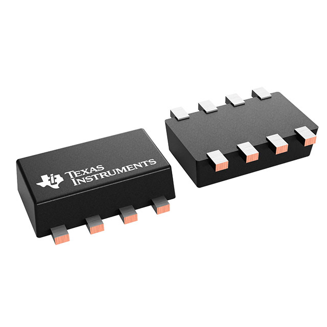
TPS629203QDRLRQ1
ActiveAUTOMOTIVE 3-V TO 17-V, 0.3-A, LOW-IQ, SYNCHRONOUS BUCK CONVERTER IN SOT-583 PACKAGE
Deep-Dive with AI
Search across all available documentation for this part.

TPS629203QDRLRQ1
ActiveAUTOMOTIVE 3-V TO 17-V, 0.3-A, LOW-IQ, SYNCHRONOUS BUCK CONVERTER IN SOT-583 PACKAGE
Deep-Dive with AI
Technical Specifications
Parameters and characteristics for this part
| Specification | TPS629203QDRLRQ1 |
|---|---|
| Current - Output | 300 mA |
| Frequency - Switching | 2.5 MHz, 1 MHz |
| Function | Step-Down |
| Grade | Automotive |
| Mounting Type | Surface Mount |
| Number of Outputs | 1 |
| Operating Temperature [Max] | 150 °C |
| Operating Temperature [Min] | -40 °C |
| Output Configuration | Positive |
| Output Type | Adjustable |
| Package / Case | SOT-583 |
| Qualification | AEC-Q100 |
| Supplier Device Package | SOT-583 |
| Synchronous Rectifier | True |
| Topology | Buck |
| Voltage - Input (Max) [Max] | 17 V |
| Voltage - Input (Min) [Min] | 3 V |
| Voltage - Output (Max) [Max] | 5.5 V |
| Voltage - Output (Min/Fixed) [Min] | 0.4 V |
Pricing
Prices provided here are for design reference only. For realtime values and availability, please visit the distributors directly
| Distributor | Package | Quantity | $ | |
|---|---|---|---|---|
| Digikey | Cut Tape (CT) | 1 | $ 2.15 | |
| 10 | $ 1.38 | |||
| 25 | $ 1.17 | |||
| 100 | $ 0.94 | |||
| 250 | $ 0.83 | |||
| 500 | $ 0.76 | |||
| 1000 | $ 0.70 | |||
| Digi-Reel® | 1 | $ 2.15 | ||
| 10 | $ 1.38 | |||
| 25 | $ 1.17 | |||
| 100 | $ 0.94 | |||
| 250 | $ 0.83 | |||
| 500 | $ 0.76 | |||
| 1000 | $ 0.70 | |||
| N/A | 2783 | $ 1.27 | ||
| Tape & Reel (TR) | 4000 | $ 0.51 | ||
| 8000 | $ 0.48 | |||
| 12000 | $ 0.47 | |||
| 20000 | $ 0.45 | |||
| Mouser | N/A | 1 | $ 1.27 | |
| 10 | $ 0.92 | |||
| 25 | $ 0.83 | |||
| 100 | $ 0.74 | |||
| 250 | $ 0.69 | |||
| 500 | $ 0.67 | |||
| 1000 | $ 0.60 | |||
| 4000 | $ 0.49 | |||
| 8000 | $ 0.47 | |||
| Texas Instruments | LARGE T&R | 1 | $ 0.88 | |
| 100 | $ 0.68 | |||
| 250 | $ 0.50 | |||
| 1000 | $ 0.36 | |||
Description
General part information
TPS629203 Series
The automotive-qualified TPS6292xx -Q1 family of devices are highly efficient, small, and highly flexible synchronous step-down DC-DC converter s that are easy to use. A wide 3-V to 1 7-V input voltage range supports a wide variety of systems powered from either 12-V, 5-V, or 3.3-V supply rails, or single-cell or multi-cell Li-Ion batteries. The TPS629203-Q1 can be configured to run at either 2.5 MHz or 1 MHz in a forced PWM mode or a variable frequency (auto PFM) mode. In auto PFM mode, the device automatically transitions to power save mode at light loads to maintain high efficiency. The low 4-µA typical quiescent current also provides high efficiency down to the smallest loads. TI’s automatic efficiency enhancement (AEE) mode holds a high conversion efficiency through the whole operation range without the need of using different inductors by automatically adjusting the switching frequency based on input and output voltages. In addition to selecting the switching frequency behavior, the MODE/S-CONF input pin can also be used to select between different combinations of external and internal feedback dividers and enabling and disabling the output voltage discharge capability. In the internal feedback configuration, a resistor between the FB/VSET pin and GND can be used to select between 18 different output voltage options (see Table 8-2).
The automotive-qualified TPS6292xx -Q1 family of devices are highly efficient, small, and highly flexible synchronous step-down DC-DC converter s that are easy to use. A wide 3-V to 1 7-V input voltage range supports a wide variety of systems powered from either 12-V, 5-V, or 3.3-V supply rails, or single-cell or multi-cell Li-Ion batteries. The TPS629203-Q1 can be configured to run at either 2.5 MHz or 1 MHz in a forced PWM mode or a variable frequency (auto PFM) mode. In auto PFM mode, the device automatically transitions to power save mode at light loads to maintain high efficiency. The low 4-µA typical quiescent current also provides high efficiency down to the smallest loads. TI’s automatic efficiency enhancement (AEE) mode holds a high conversion efficiency through the whole operation range without the need of using different inductors by automatically adjusting the switching frequency based on input and output voltages. In addition to selecting the switching frequency behavior, the MODE/S-CONF input pin can also be used to select between different combinations of external and internal feedback dividers and enabling and disabling the output voltage discharge capability. In the internal feedback configuration, a resistor between the FB/VSET pin and GND can be used to select between 18 different output voltage options (see Table 8-2).


