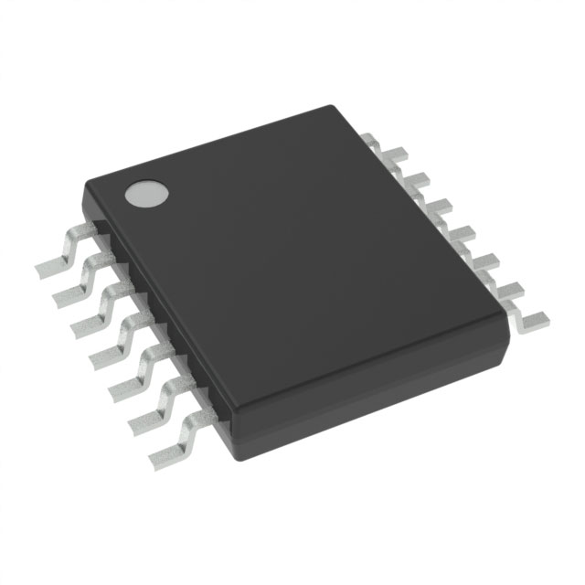
SN74LVC06APWT
Active6-CH, 1.65-V TO 3.6-V INVERTERS WITH OPEN-DRAIN OUTPUTS
Deep-Dive with AI
Search across all available documentation for this part.

SN74LVC06APWT
Active6-CH, 1.65-V TO 3.6-V INVERTERS WITH OPEN-DRAIN OUTPUTS
Deep-Dive with AI
Technical Specifications
Parameters and characteristics for this part
| Specification | SN74LVC06APWT |
|---|---|
| Current - Output High, Low [custom] | 24 mA |
| Current - Output High, Low [custom] | - |
| Current - Quiescent (Max) [Max] | 1 çA |
| Features | Open Drain |
| Input Logic Level - High [Max] | 2 V |
| Input Logic Level - High [Min] | 1.7 V |
| Input Logic Level - Low [Max] | 0.8 V |
| Input Logic Level - Low [Min] | 0.7 V |
| Logic Type | Inverter |
| Max Propagation Delay @ V, Max CL | 3.5 ns |
| Mounting Type | Surface Mount |
| Number of Circuits | 6 |
| Number of Inputs | 1 |
| Operating Temperature [Max] | 125 °C |
| Operating Temperature [Min] | -40 °C |
| Package / Case | 14-TSSOP |
| Package / Case [custom] | 0.173 " |
| Package / Case [custom] | 4.4 mm |
| Supplier Device Package | 14-TSSOP |
| Voltage - Supply [Max] | 3.6 V |
| Voltage - Supply [Min] | 1.65 V |
Pricing
Prices provided here are for design reference only. For realtime values and availability, please visit the distributors directly
| Distributor | Package | Quantity | $ | |
|---|---|---|---|---|
| Digikey | Cut Tape (CT) | 1 | $ 1.02 | |
| 10 | $ 0.91 | |||
| 25 | $ 0.86 | |||
| 100 | $ 0.71 | |||
| Digi-Reel® | 1 | $ 1.02 | ||
| 10 | $ 0.91 | |||
| 25 | $ 0.86 | |||
| 100 | $ 0.71 | |||
| Tape & Reel (TR) | 250 | $ 0.47 | ||
| 500 | $ 0.41 | |||
| 1250 | $ 0.38 | |||
| Texas Instruments | SMALL T&R | 1 | $ 0.88 | |
| 100 | $ 0.59 | |||
| 250 | $ 0.46 | |||
| 1000 | $ 0.30 | |||
Description
General part information
SN74LVC06A-Q1 Series
The SN74LVC06A is a hex inverter buffer/driver that is designed for 1.65-V to 3.6-V VCCoperation.
The outputs of the SN74LVC06A device are open drain and can be connected to other open-drain outputs to implement active low wired OR or active high wired AND functions. The maximum sink current is 24 mA.
Inputs can be driven from either 3.3 V or 5 V devices. This feature allows the use of these devices as translators in a mixed 3.3 V/5 V system environment.
Documents
Technical documentation and resources


