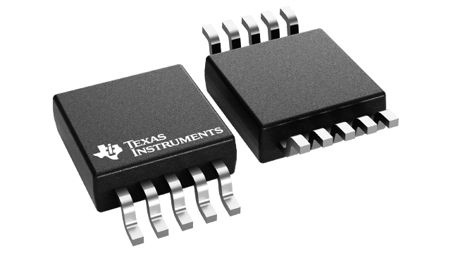
TPS60310DGS
ActiveSINGLE-CELL TO 3.3-V, 20-MA ULTRA-LOW QUIESCENT CURRENT CHARGE PUMP AND OPEN-DRAIN POWER-GOOD OUTPUT
Deep-Dive with AI
Search across all available documentation for this part.

TPS60310DGS
ActiveSINGLE-CELL TO 3.3-V, 20-MA ULTRA-LOW QUIESCENT CURRENT CHARGE PUMP AND OPEN-DRAIN POWER-GOOD OUTPUT
Deep-Dive with AI
Technical Specifications
Parameters and characteristics for this part
| Specification | TPS60310DGS |
|---|---|
| Current - Output | 40 mA, 20 mA |
| Frequency - Switching | 700 kHz |
| Function | Step-Up, Ratiometric |
| Mounting Type | Surface Mount |
| Number of Outputs | 2 |
| Operating Temperature [Max] | 125 ¯C |
| Operating Temperature [Min] | -40 °C |
| Output Configuration | Positive |
| Output Type | 1.81 mOhm |
| Package / Case | 10-MSOP, 10-TFSOP |
| Package / Case [x] | 3 mm |
| Package / Case [x] | 0.118 in |
| Supplier Device Package | 10-VSSOP |
| Synchronous Rectifier | False |
| Voltage - Input (Max) [Max] | 1.8 V |
| Voltage - Input (Min) [Min] | 0.9 V |
| Voltage - Output (Min/Fixed) | 3.3 V |
| Voltage - Output (Min/Fixed) | 2Vin |
Pricing
Prices provided here are for design reference only. For realtime values and availability, please visit the distributors directly
| Distributor | Package | Quantity | $ | |
|---|---|---|---|---|
| Digikey | Tube | 1 | $ 3.74 | |
| 10 | $ 2.46 | |||
| 25 | $ 2.12 | |||
| 100 | $ 1.74 | |||
| 250 | $ 1.56 | |||
| Texas Instruments | TUBE | 1 | $ 2.30 | |
| 100 | $ 1.90 | |||
| 250 | $ 1.36 | |||
| 1000 | $ 1.03 | |||
Description
General part information
TPS60310 Series
The TPS6031X step-up, regulated charge pumps generate a 3-V ±4% or 3.3-V ±4% output voltage from a 0.9-V to 1.8-V input voltage (one alkaline, NiCd, or NiMH battery).
Only five small 1-uF ceramic capacitors are required to build a complete high-efficiency dc/dc charge pump converter. To achieve the high efficiency over a wide input voltage range, the charge pump automatically selects between a 3x or 4x conversion mode.
Output 1 (OUT1) can deliver a maximum of 40 mA, from a 1-V input, with output 2 (OUT2) not loaded. OUT2 can deliver a maximum of 20 mA, from a 1-V input, with OUT1 not loaded. Both outputs can be loaded at the same time, but the total output current of the first voltage doubler must not exceed 40 mA. For example, the load at OUT1 is 20 mA and the load at output 2 is 10 mA.
Documents
Technical documentation and resources


