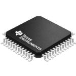
TSB14AA1APFB
ActiveIEEE 1394-1995, 3.3-V, 1-PORT, 50/100-MBPS, BACKPLANE PHY
Deep-Dive with AI
Search across all available documentation for this part.

TSB14AA1APFB
ActiveIEEE 1394-1995, 3.3-V, 1-PORT, 50/100-MBPS, BACKPLANE PHY
Deep-Dive with AI
Technical Specifications
Parameters and characteristics for this part
| Specification | TSB14AA1APFB |
|---|---|
| Function | Physical Layer Controller |
| Operating Temperature [Max] | 70 °C |
| Operating Temperature [Min] | 0 °C |
| Package / Case | 48-TQFP |
| Protocol | IEEE 1394 |
| Standards | IEEE 1394-1995 |
| Supplier Device Package | 48-TQFP (7x7) |
| Voltage - Supply | 3.3 V |
Pricing
Prices provided here are for design reference only. For realtime values and availability, please visit the distributors directly
| Distributor | Package | Quantity | $ | |
|---|---|---|---|---|
| Digikey | N/A | 0 | $ 11.21 | |
| 50247 | $ 11.21 | |||
| Tray | 250 | $ 9.35 | ||
| Texas Instruments | JEDEC TRAY (10+1) | 1 | $ 10.51 | |
| 100 | $ 9.18 | |||
| 250 | $ 7.08 | |||
| 1000 | $ 6.33 | |||
Description
General part information
TSB14AA1 Series
The TSB14AA1A (TSB14AA1A refers to all three devices: TSB14AA1A, TSB14AA1AI, and TSB14AA1AT) is the second-generation 1394 backplane physical layer device. It is recommended for use in all new designs instead of the first generation TSB14C01A. It provides the physical layer functions needed to implement a single port node in a backplane based 1394 network. The TSB14AA1A provides two pins for transmitting, two for receiving, and two pins to externally control the transceivers for data and strobe. In addition to supporting open-collector drivers, the TSB14AA1A can also support 3-state(1)(high-impedance) drivers. The TSB14AA1A is not designed to drive the backplane directly; this function must be provided externally. The TSB14AA1A is designed to interface with a link-layer controller (LLC), such as the TSB12LV01B, TSB12LV32, TSB12LV21B, etc.
The TSB14AA1A requires an external 98.304-MHz reference oscillator input for S100 asynchronous only operation or 49.152-MHz for S50 asynchronous only operation. Two clock select pins (CLK_SEL0, CLK_SEL1) select the speed mode for the TSB14AA1A (see Table 1-1). For S100 operation, the 98.304-MHz reference signal is internally divided to provide the 49.152-MHz system clock signals used to control transmission of the outbound encoded strobe and data information. The 49.152-MHz clock signal is also supplied to the associated LLC for synchronization of the two chips and is used for resynchronization of the received data. For S50 operation, a 49.152-MHz reference signal is used. This reference signal is internally divided to provide the 24.576-MHz system clock signals for S50 operations.
During packet transmit, data bits to be transmitted are received from the LLC on two parallel paths and are latched internally in the TSB14AA1A in synchronization with the system clock. These bits are combined serially, encoded, and transmitted as the outbound data-strobe information stream. During transmit, the encoded data information is transmitted on TDATA, and the encoded strobe information is transmitted on TSTRB.
Documents
Technical documentation and resources


