Zenode.ai Logo
Beta
Product thumbnail image
Integrated Circuits (ICs)

BD9227F-E2

Active
Rohm Semiconductor

6V TO 20V, 1A 1CH PWM BUCK CONVERTER WITH AN INTEGRATED FET

Deep-Dive with AI

Search across all available documentation for this part.

Product thumbnail image
Integrated Circuits (ICs)

BD9227F-E2

Active
Rohm Semiconductor

6V TO 20V, 1A 1CH PWM BUCK CONVERTER WITH AN INTEGRATED FET

Technical Specifications

Parameters and characteristics for this part

SpecificationBD9227F-E2
Current - Output1 A
Frequency - Switching1 MHz
FunctionStep-Down
Mounting TypeSurface Mount
Number of Outputs1
Operating Temperature [Max]85 °C
Operating Temperature [Min]-40 °C
Output ConfigurationPositive
Output TypeAdjustable
Package / Case0.173 in
Package / Case4.4 mm
Package / Case8-SOIC
Supplier Device Package8-SOP
Synchronous RectifierFalse
TopologyBuck
Voltage - Input (Max) [Max]20 V
Voltage - Input (Min) [Min]6 V
Voltage - Output (Max) [Max]20 V
Voltage - Output (Min/Fixed)1.512 V

Pricing

Prices provided here are for design reference only. For realtime values and availability, please visit the distributors directly

DistributorPackageQuantity$
DigikeyCut Tape (CT) 1$ 2.26
10$ 1.45
25$ 1.24
100$ 1.00
250$ 0.88
500$ 0.81
1000$ 0.75
Digi-Reel® 1$ 2.26
10$ 1.45
25$ 1.24
100$ 1.00
250$ 0.88
500$ 0.81
1000$ 0.75
Tape & Reel (TR) 2500$ 0.58
5000$ 0.55
7500$ 0.53
12500$ 0.51
17500$ 0.50
NewarkEach (Supplied on Cut Tape) 1$ 1.62
10$ 1.12
25$ 1.03
50$ 0.95
100$ 0.86
250$ 0.82
500$ 0.78
1000$ 0.71

Description

General part information

BD9227F Series

The BD9227F is a 20V, 1A non-synchronous PWM duty control buck converter with an integrated internal high-side 20V Power MOSFET. Operating frequency is 1.0MHz fixed by inner circuit. Current mode control with internal slope compensation simplifies the external compensation calculation and reduces component count while allowing the use of ceramic output capacitors. Additional protection features are included such as Over Current Protection, Thermal Shutdown and Under Voltage Lockout. The under voltage lockout and hysteresis can be set by an external resistor. The BD9227F is available in SOP8.

Documents

Technical documentation and resources

UL94 Flame Classifications of Mold Compound

Environmental Data

θ<sub>JA</sub> and Ψ<sub>JT</sub>

Thermal Design

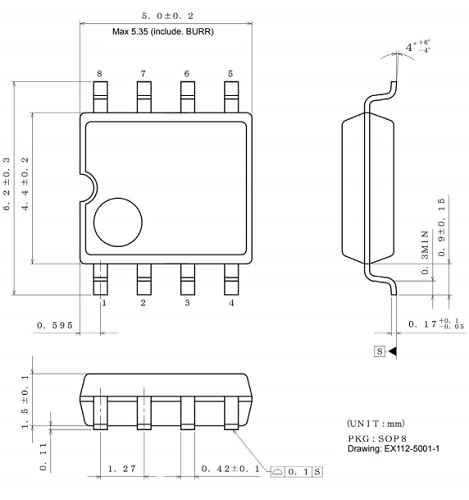
SOP8 Package Information

Package Information

Method for Calculating Junction Temperature from Transient Thermal Resistance Data

Thermal Design

Considering Input Filter to Reduce Conducted Emissions by DCDC Converter

Schematic Design & Verification

Snubber Circuit for Buck Converter IC

Schematic Design & Verification

Thermal Resistance

Thermal Design

Power Supply Sequence Circuit with General Purpose Power Supply IC

Schematic Design & Verification

Capacitor Calculation for Buck converter IC

Schematic Design & Verification

Cutting-Edge Web Simulation Tool "ROHM Solution Simulator" Capable of Complete Circuit Verification of Power Devices and Driver ICs

White Paper

Efficiency of Buck Converter

Schematic Design & Verification

Compliance with the ELV directive

Environmental Data

Impedance Characteristics of Bypass Capacitor

Schematic Design & Verification

What Is Thermal Design

Thermal Design

Three Steps for Successful Design of DC-DC Converters

White Paper

Method for Determining Constants of Peripheral Parts of Buck DC/DC Converter

Schematic Design & Verification

PCB Layout Thermal Design Guide

Thermal Design

Factory Information

Manufacturing Data

Solder Joint Rate and Thermal Resistance of Exposed Pad

Thermal Design

Overview of ROHM's Simulation Models(for ICs and Discrete Semiconductors)

Technical Article

PCB Layout Techniques of Buck Converter

Schematic Design & Verification

Types of Capacitors Used for Output Smoothing of Switching Regulators and their Precautions

Schematic Design & Verification

Five Steps for Successful Thermal Design of IC

White Paper

Considerations for Power Inductors Used for Buck Converters

Schematic Design & Verification

Two-Resistor Model for Thermal Simulation

Thermal Design

Suppression Method of Switching Noise Using Linear Regulator and Low Pass Filter

Schematic Design & Verification

Design Guide and Example of Stencil for Exposed Pad

Thermal Design

PCB Layout Essential Check sheet for Switching Regulator

Schematic Design & Verification

Resistor Value Table to set Output Voltage of Buck Converter IC

Schematic Design & Verification

The Important Points of Multi-layer Ceramic Capacitor Used in Buck Converter circuit

Schematic Design & Verification

Precautions for PCB Layout Regarding Common Mode Filters

Technical Article

Judgment Criteria of Thermal Evaluation

Thermal Design

Phase Compensation Design for Current Mode Buck Converter

Schematic Design & Verification

How to Use the Thermal Resistance and Thermal Characteristics Parameters

Thermal Design

Calculation of Power Loss (Synchronous)

Schematic Design & Verification

Anti-Whisker formation

Package Information

Step-down DC-DC converter PCB layout EMC Design guide

Schematic Design & Verification

Considering Polarity of Power Inductor to Reduce Radiated Emission of DC-DC converter

Schematic Design & Verification

Measurement Method for Phase Margin with Frequency Response Analyzer (FRA)

Schematic Design & Verification

Heat Dissipation Effect of Thermal Via in Exposed Pad Type Package

Thermal Design