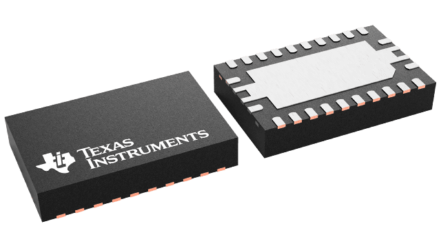
CLVC8T245MRHLTEP
ActiveENHANCED PRODUCT 8-BIT DUAL-SUPPLY BUS TRANSC. W/ CONFIGURABLE VOLTAGE TRANSL., AND 3-STATE OUTPUTS
Deep-Dive with AI
Search across all available documentation for this part.

CLVC8T245MRHLTEP
ActiveENHANCED PRODUCT 8-BIT DUAL-SUPPLY BUS TRANSC. W/ CONFIGURABLE VOLTAGE TRANSL., AND 3-STATE OUTPUTS
Technical Specifications
Parameters and characteristics for this part
| Specification | CLVC8T245MRHLTEP |
|---|---|
| Current - Output High, Low [x] | 32 mA |
| Current - Output High, Low [y] | 32 mA |
| Logic Type | Translation Transceiver |
| Mounting Type | Surface Mount |
| Number of Bits per Element | 8 |
| Number of Elements | 1 |
| Operating Temperature [Max] | 125 °C |
| Operating Temperature [Min] | -55 °C |
| Output Type | 3-State |
| Package / Case | 24-VFQFN Exposed Pad |
| Supplier Device Package | 24-VQFN |
| Supplier Device Package [x] | 5.5 |
| Supplier Device Package [y] | 3.5 |
| Voltage - Supply [Max] | 5.5 V |
| Voltage - Supply [Min] | 1.65 V |
Pricing
Prices provided here are for design reference only. For realtime values and availability, please visit the distributors directly
| Distributor | Package | Quantity | $ | |
|---|---|---|---|---|
| Digikey | Cut Tape (CT) | 1 | $ 9.98 | |
| 10 | $ 6.94 | |||
| 25 | $ 6.15 | |||
| 100 | $ 5.27 | |||
| Digi-Reel® | 1 | $ 9.98 | ||
| 10 | $ 6.94 | |||
| 25 | $ 6.15 | |||
| 100 | $ 5.27 | |||
| Tape & Reel (TR) | 250 | $ 4.85 | ||
| 500 | $ 4.59 | |||
| 750 | $ 4.46 | |||
| 1250 | $ 4.31 | |||
| 1750 | $ 4.29 | |||
| Texas Instruments | SMALL T&R | 1 | $ 7.22 | |
| 100 | $ 5.89 | |||
| 250 | $ 4.63 | |||
| 1000 | $ 3.92 | |||
Description
General part information
SN74LVC8T245-EP Series
The SN74LVC8T245 is an eight bit non-inverting bus transceiver with configurable dual power supply rails that enables bidirectional voltage level translation. The SN74LVC8T245 is optimized to operate with V CCA and V CCB set at 1.65 V to 5.5 V. The A port is designed to track V CCA. V CCA accepts any supply voltage from 1.65 V to 5.5 V. The B port is designed to track V CCB. V CCB accepts any supply voltage from 1.65 V to 5.5 V. This allows for universal low-voltage bidirectional translation between any of the 1.8-V, 2.5-V, 3.3-V, and 5.5-V voltage nodes.
The SN74LVC8T245 is designed for asynchronous communication between two data buses. The logic levels of the direction-control (DIR) input and the output-enable ( OE) input activate either the B-port outputs or the A-port outputs or place both output ports into the high-impedance mode. The device transmits data from the A bus to the B bus when the B-port outputs are activated, and from the B bus to the A bus when the A-port outputs are activated. The input circuitry on both A and B ports is always active and must have a logic HIGH or LOW level applied to prevent excess I CC and I CCZ.
This device is fully specified for partial-power-down applications using I off. The I off circuitry disables the outputs, preventing damaging current backflow through the device when it is powered down. The V CC isolation feature ensures that if either V CC input is at GND, all outputs are in the high-impedance state. To ensure the high-impedance state during power up or power down, OE should be tied to V CC through a pullup resistor; the minimum value of the resistor is determined by the current-sinking capability of the driver.
Documents
Technical documentation and resources


