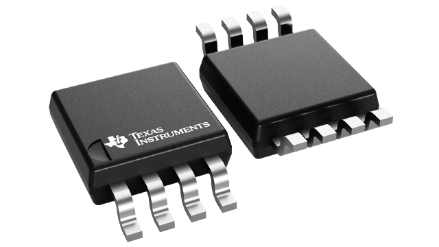
DAC8552IDGKT
Active16-BIT, DUAL-CHANNEL, ULTRALOW GLITCH, VOLTAGE OUTPUT, DIGITAL TO ANALOG CONVERTER
Deep-Dive with AI
Search across all available documentation for this part.

DAC8552IDGKT
Active16-BIT, DUAL-CHANNEL, ULTRALOW GLITCH, VOLTAGE OUTPUT, DIGITAL TO ANALOG CONVERTER
Technical Specifications
Parameters and characteristics for this part
| Specification | DAC8552IDGKT |
|---|---|
| Architecture | String DAC |
| Data Interface | DSP, SPI |
| Differential Output | False |
| INL/DNL (LSB) | |
| Mounting Type | Surface Mount |
| Number of Bits | 16 |
| Operating Temperature [Max] | 105 ░C |
| Operating Temperature [Min] | -40 °C |
| Output Type | Voltage - Buffered |
| Package / Case | 8-MSOP, 8-TSSOP |
| Package / Case | 3 mm |
| Package / Case [custom] | 0.118 in |
| Reference Type | External |
| Settling Time | 10 µs |
| Voltage - Supply, Analog [Max] | 5.5 V |
| Voltage - Supply, Analog [Min] | 2.7 V |
| Voltage - Supply, Digital [Max] | 5.5 V |
| Voltage - Supply, Digital [Min] | 2.7 V |
Pricing
Prices provided here are for design reference only. For realtime values and availability, please visit the distributors directly
| Distributor | Package | Quantity | $ | |
|---|---|---|---|---|
| Digikey | Cut Tape (CT) | 1 | $ 10.96 | |
| 10 | $ 9.90 | |||
| 25 | $ 9.44 | |||
| 100 | $ 8.20 | |||
| Digi-Reel® | 1 | $ 10.96 | ||
| 10 | $ 9.90 | |||
| 25 | $ 9.44 | |||
| 100 | $ 8.20 | |||
| Tape & Reel (TR) | 250 | $ 7.83 | ||
| 500 | $ 7.14 | |||
| 1250 | $ 6.22 | |||
| Texas Instruments | SMALL T&R | 1 | $ 8.39 | |
| 100 | $ 6.84 | |||
| 250 | $ 5.38 | |||
| 1000 | $ 4.56 | |||
Description
General part information
DAC8552 Series
The DAC8552 is a 16-bit, dual channel, voltage output digital-to-analog converter (DAC) offering low power operation and a flexible serial host interface. Each on-chip precision output amplifier allows rail-to-rail output swing to be achieved over the supply range of 2.7V to 5.5V. The device supports a standard 3-wire serial interface capable of operating with input data clock frequencies up to 30MHz for VDD= 5V.
The DAC8552 requires an external reference voltage to set the output range of each DAC channel. Also incorporated into the device is a power-on reset circuit which ensures that the DAC outputs power up at zero-scale and remain there until a valid write takes place. The DAC8552 provides a flexible power-down feature, accessed over the serial interface, that reduces the current consumption of the device to 700nA at 5V.
The low-power consumption of this device in normal operation makes it ideally suited for portable, battery-operated equipment and other low-power applications. The power consumption is 0.5mW per channel at 2.7V, reducing to 1µW in power-down mode.
Documents
Technical documentation and resources


