Deep-Dive with AI
Search across all available documentation for this part.

Deep-Dive with AI
Technical Specifications
Parameters and characteristics for this part
| Specification | TPS61121PWRG4 |
|---|---|
| Applications | Handheld/Mobile Devices |
| Current - Supply | 10 µA |
| Mounting Type | Surface Mount |
| Operating Temperature [Max] | 85 °C |
| Operating Temperature [Min] | -40 °C |
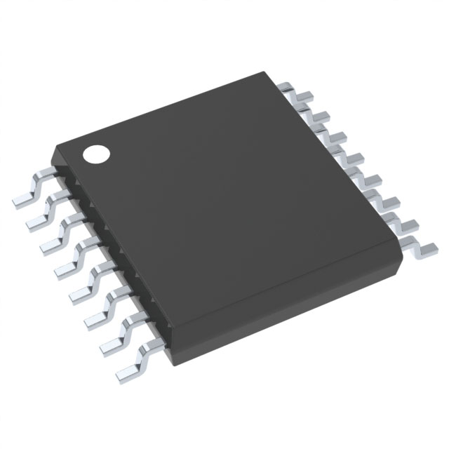
| Package / Case | 16-TSSOP |
| Package / Case [x] | 0.173 in |
| Package / Case [y] | 4.4 mm |
| Supplier Device Package | 16-TSSOP |
| Voltage - Supply [Max] | 5.5 V |
| Voltage - Supply [Min] | 1.8 V |
Pricing
Prices provided here are for design reference only. For realtime values and availability, please visit the distributors directly
| Distributor | Package | Quantity | $ | |
|---|---|---|---|---|
Description
General part information
TPS61121 Series
The TPS6112x devices provide a complete power supply solution for products powered by either a one-cell Li-Ion or Li-Polymer by either a one-cell Li-Ion or Li-Polymer battery, or a two- to four-cell Alkaline, NiCd, or NiMH battery. The devices can generate two stable output voltages that are either adjusted by an external resistor divider or are fixed internally on the chip. The device also provides a simple solution for generating 3.3 V out of a one-cell Li-Ion or Li-Polymer battery at a maximum output current of at least 200 mA with supply voltages down to 1.8 V. The implemented boost converter is based on a fixed frequency, pulse-width-modulation (PWM) controller using a synchronous rectifier to obtain maximum efficiency. The maximum peak current in the boost switch is limited to a value of 1600 mA.
The converter can be disabled to minimize battery drain. During shutdown, the load is completely disconnected from the battery. A low-EMI mode is implemented to reduce ringing and, in effect, lower radiated electromagnetic energy when the converter enters discontinuous conduction mode. A power good output at the boost stage simplifies control of any connected circuits like cascaded power supply stages or microprocessors.
The built-in LDO can be used for a second output voltage derived either from the boost output or directly from the battery. The LDO can be enabled separately that is, using the power good of the boost stage. The device is packaged in a 16-pin VQFN (RSA) package measuring 4 mm × 4 mm or in a 16-pin TSSOP (PW) package.
Documents
Technical documentation and resources