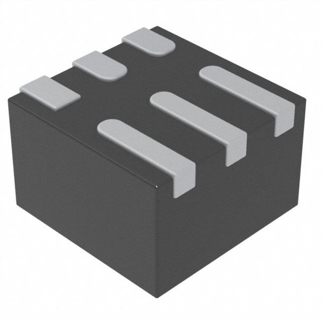
TPS6282518DMQR
Active2.4-V TO 5.5-V INPUT, 2-A STEP-DOWN CONVERTER WITH 1% ACCURACY IN 1.5-MM X 1.5-MM QFN
Deep-Dive with AI
Search across all available documentation for this part.

TPS6282518DMQR
Active2.4-V TO 5.5-V INPUT, 2-A STEP-DOWN CONVERTER WITH 1% ACCURACY IN 1.5-MM X 1.5-MM QFN
Deep-Dive with AI
Technical Specifications
Parameters and characteristics for this part
| Specification | TPS6282518DMQR |
|---|---|
| Current - Output | 2 A |
| Frequency - Switching | 2.2 MHz |
| Function | Step-Down |
| Mounting Type | Surface Mount |
| Number of Outputs | 1 |
| Operating Temperature [Max] | 125 °C |
| Operating Temperature [Min] | -40 C |
| Output Configuration | Positive |
| Package / Case | 6-VFDFN |
| Supplier Device Package | 6-VSON-HR |
| Supplier Device Package [x] | 1.5 |
| Supplier Device Package [y] | 1.5 |
| Synchronous Rectifier | True |
| Topology | Buck |
| Voltage - Input (Max) [Max] | 5.5 V |
| Voltage - Input (Min) [Min] | 2.4 V |
| Voltage - Output (Min/Fixed) | 1.8 V |
TPS62825 Series
2.4-V to 5.5-V input, 2-A step-down converter with forced PWM in 1.5-mm × 1.5-mm VSON-HR package
| Part | Output Configuration | Supplier Device Package [x] | Supplier Device Package | Supplier Device Package [y] | Mounting Type | Number of Outputs | Topology | Function | Voltage - Output (Min/Fixed) | Synchronous Rectifier | Voltage - Input (Max) [Max] | Frequency - Switching | Voltage - Input (Min) [Min] | Package / Case | Operating Temperature [Min] | Operating Temperature [Max] | Current - Output | Voltage - Output (Max) [Max] | Output Type | Outputs and Type | Outputs and Type | Supplied Contents | Board Type | Contents | Regulator Topology | Voltage - Output | Utilized IC / Part | Main Purpose | Voltage - Input [Min] | Voltage - Input [Max] |
|---|---|---|---|---|---|---|---|---|---|---|---|---|---|---|---|---|---|---|---|---|---|---|---|---|---|---|---|---|---|---|
Texas Instruments | Positive | 1.5 | 6-VSON-HR | 1.5 | Surface Mount | 1 | Buck | Step-Down | 1.8 V | 5.5 V | 2.2 MHz | 2.4 V | 6-VFDFN | -40 C | 125 °C | 2 A | ||||||||||||||
Texas Instruments | Positive | 1.5 | 6-VSON-HR | 1.5 | Surface Mount | 1 | Buck | Step-Down | 3.3 V | 5.5 V | 2.2 MHz | 2.4 V | 6-VFDFN | -40 C | 125 °C | 2 A | ||||||||||||||
Texas Instruments | Positive | 1.5 | 6-VSON-HR | 1.5 | Surface Mount | 1 | Buck | Step-Down | 1.8 V | 5.5 V | 2.2 MHz | 2.4 V | 6-VFDFN | -40 C | 125 °C | 2 A | ||||||||||||||
Texas Instruments | Positive | 1.5 | 6-VSON-HR | 1.5 | Surface Mount | 1 | Buck | Step-Down | 0.6 V | 5.5 V | 2.2 MHz | 2.4 V | 6-VFDFN | -40 C | 125 °C | 2 A | 4 V | Adjustable | ||||||||||||
Texas Instruments | Positive | 1.5 | 6-VSON-HR | 1.5 | Surface Mount | 1 | Buck | Step-Down | 0.6 V | 5.5 V | 2.2 MHz | 2.4 V | 6-VFDFN | -40 C | 125 °C | 2 A | 4 V | Adjustable | ||||||||||||
Texas Instruments | 2.2 MHz | 2 A | 1 | 1 Non-Isolated Output Non-Isolated | Board(s) | Fully Populated | Board(s) | Buck | 1.8 V | TPS62825A | DC/DC Step Down | 2.4 V | 5.5 V | |||||||||||||||||
Texas Instruments | 2.2 MHz | 2 A | 1 | 1 Non-Isolated Output Non-Isolated | Board(s) | Fully Populated | Board(s) | Buck | 1.8 V | TPS62825 | DC/DC Step Down | 2.4 V | 5.5 V | |||||||||||||||||
Texas Instruments | Positive | 1.5 | 6-VSON-HR | 1.5 | Surface Mount | 1 | Buck | Step-Down | 0.6 V | 5.5 V | 2.2 MHz | 2.4 V | 6-VFDFN | -40 C | 125 °C | 2 A | 4 V | Adjustable |
Pricing
Prices provided here are for design reference only. For realtime values and availability, please visit the distributors directly
| Distributor | Package | Quantity | $ | |
|---|---|---|---|---|
| Digikey | Cut Tape (CT) | 1 | $ 1.17 | |
| 10 | $ 1.04 | |||
| 25 | $ 0.99 | |||
| 100 | $ 0.81 | |||
| 250 | $ 0.76 | |||
| 500 | $ 0.67 | |||
| 1000 | $ 0.53 | |||
| Digi-Reel® | 1 | $ 1.17 | ||
| 10 | $ 1.04 | |||
| 25 | $ 0.99 | |||
| 100 | $ 0.81 | |||
| 250 | $ 0.76 | |||
| 500 | $ 0.67 | |||
| 1000 | $ 0.53 | |||
| N/A | 7669 | $ 1.25 | ||
| Tape & Reel (TR) | 3000 | $ 0.49 | ||
| 6000 | $ 0.47 | |||
| 15000 | $ 0.45 | |||
| Texas Instruments | LARGE T&R | 1 | $ 0.86 | |
| 100 | $ 0.67 | |||
| 250 | $ 0.49 | |||
| 1000 | $ 0.35 | |||
Description
General part information
TPS62825 Series
The TPS6282x is an easy-to-use, synchronous step-down DC/DC converters family with a very low quiescent current of only 4µA. Based on the DCS-Control topology, the device provides a fast transient response. The internal reference allows to regulate the output voltage down to 0.6V with a high feedback voltage accuracy of 1% over the junction temperature range of –40°C to 125°C. The family devices are pin-to-pin and BOM-to-BOM compatible. The entire design requires a small 470nH inductor, a single 4.7µF input capacitor, and two 10µF or single 22µF output capacitor.
The TPS6282x is available in two flavors. The first includes an automatically entered power save mode to maintain high efficiency down to very light loads for extending the system battery run-time. The second runs in forced-PWM maintaining a continuous conduction mode to make sure of the least ripple in the output voltage and a quasi-fixed switching frequency. The device features a Power-Good signal and an internal soft-start circuit. The device is able to operate in 100% mode. For fault protection, the device incorporates a HICCUP short-circuit protection as well as a thermal shutdown. The device is available in a 6-pin 1.5mm × 1.5mm QFN package, offering the highest power density design.
The TPS6282x is an easy-to-use, synchronous step-down DC/DC converters family with a very low quiescent current of only 4µA. Based on the DCS-Control topology, the device provides a fast transient response. The internal reference allows to regulate the output voltage down to 0.6V with a high feedback voltage accuracy of 1% over the junction temperature range of –40°C to 125°C. The family devices are pin-to-pin and BOM-to-BOM compatible. The entire design requires a small 470nH inductor, a single 4.7µF input capacitor, and two 10µF or single 22µF output capacitor.
Documents
Technical documentation and resources


