5V2305NRGI
Active2.5V TO 3.3V HIGH PERFORMANCE CLOCK BUFFER
Deep-Dive with AI
Search across all available documentation for this part.

5V2305NRGI
Active2.5V TO 3.3V HIGH PERFORMANCE CLOCK BUFFER
Deep-Dive with AI
Technical Specifications
Parameters and characteristics for this part
| Specification | 5V2305NRGI |
|---|---|
| Differential - Input:Output [custom] | False |
| Differential - Input:Output [custom] | False |
| Frequency - Max [Max] | 200 MHz |
| Input | LVCMOS, LVTTL |
| Mounting Type | Surface Mount |
| Number of Circuits | 1 |
| Operating Temperature [Max] | 85 °C |
| Operating Temperature [Min] | -40 C |
| Output | LVCMOS |
| Package / Case | 16-VFQFN Exposed Pad |
| Ratio - Input:Output | 1:5 |
| Supplier Device Package | 16-VFQFPN (3.5x4) |
| Type | Fanout Buffer (Distribution) |
| Voltage - Supply [Max] | 3.6 V |
| Voltage - Supply [Min] | 2.3 V |
Pricing
Prices provided here are for design reference only. For realtime values and availability, please visit the distributors directly
| Distributor | Package | Quantity | $ | |
|---|---|---|---|---|
| Digikey | N/A | 425 | $ 3.62 | |
| Strip | 1 | $ 3.83 | ||
| 10 | $ 3.44 | |||
| 25 | $ 3.25 | |||
| 100 | $ 2.82 | |||
| 250 | $ 2.67 | |||
| 500 | $ 2.40 | |||
| 1000 | $ 2.02 | |||
| 2500 | $ 1.92 | |||
| 5000 | $ 1.85 | |||
Description
General part information
5V2305 Series
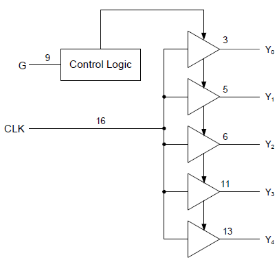
The IDT5V2305 is a high performance, low skew clock buffer that operates up to 200MHz. One bank of five outputs provides low skew copies of CLK. Through the use of control pin G, the outputs of bank Y(0:4) can be placed in a low state regardless of CLK input. The device operates in 2.5V and 3.3V environments. The built-in output enable glitch suppression ensures a synchronized output enable sequence to distribute full period clock signals. The IDT5V2305 is characterized for operation from -40°C to +85°C.
Documents
Technical documentation and resources


