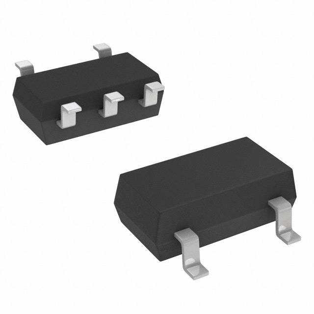
M74VHC1GT04DFT3G
ObsoleteLOGIC IC, INVERTER, SINGLE, 1 INPUTS, 5 PINS, SC-88A, 74VHC1GT04
Deep-Dive with AI
Search across all available documentation for this part.

M74VHC1GT04DFT3G
ObsoleteLOGIC IC, INVERTER, SINGLE, 1 INPUTS, 5 PINS, SC-88A, 74VHC1GT04
Deep-Dive with AI
Technical Specifications
Parameters and characteristics for this part
| Specification | M74VHC1GT04DFT3G |
|---|---|
| Current - Output High, Low [custom] | 8 mA |
| Current - Output High, Low [custom] | 8 mA |
| Current - Quiescent (Max) [Max] | 1 çA |
| Input Logic Level - High [Max] | 2 V |
| Input Logic Level - High [Min] | 1.4 V |
| Input Logic Level - Low [Max] | 0.8 V |
| Input Logic Level - Low [Min] | 0.53 V |
| Logic Type | Inverter |
| Max Propagation Delay @ V, Max CL | 7.7 ns |
| Mounting Type | Surface Mount |
| Number of Circuits | 1 |
| Number of Inputs | 1 |
| Operating Temperature [Max] | 125 °C |
| Operating Temperature [Min] | -55 °C |
| Package / Case | SC-70-5, 5-TSSOP, SOT-353 |
| Supplier Device Package | SC-88A |
| Supplier Device Package | SOT-353 |
| Supplier Device Package | SC-70-5 |
| Voltage - Supply [Max] | 5.5 V |
| Voltage - Supply [Min] | 3 V |
Pricing
Prices provided here are for design reference only. For realtime values and availability, please visit the distributors directly
| Distributor | Package | Quantity | $ | |
|---|---|---|---|---|
Description
General part information
MC74VHC1GT04 Series
The MC74VHC1GT04 is a single inverting buffer fabricated in silicon gate CMOS technology. It achieves high speed operation while maintaining CMOS low power dissipation.The internal circuit is composed of three stages, including a buffer output which provides high noise immunity and stable output.The device input is has low input threshold and the output has a full 5V CMOS level output swing. The input protection circuitry on this device is overvoltage tolerant, allowing the device to be used as a logic-level translator.The MC74VHC1GT04 input structure provides protection when voltages up to 5.5V are applied, regardless of the supply voltage, allowing the the part to be used to interface 1.8/3.3V 3/5V circuits . The output structures also provide protection when VCC= 0V.These input and output structures help prevent device destruction caused by supply voltage - input/output voltage mismatch, battery backup, hot insertion, etc.
Documents
Technical documentation and resources


